In the current interface of electronics, mixed-signal PCB design is important for modern high-performing devices. For any category of professionals, such as a PCB manufacturer, an electronics engineer, or a product designer, knowing how to enhance signal integrity in mixed-signal designs is important. This section addresses the major design concerns while presenting ways to achieve reliable performance.
What do you mean by Mixed-Signal Design?
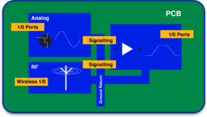
A mixed-signal PCB combines an analog and digital integration on a single board. This creates challenges such as noise from other sources, routing signals, and creating a ground. Good design techniques assist in achieving adequate, reliable, and efficient functionality, ensuring that both signal types exist without interfering with one another.
Steps to create an efficient Mixed-Signal PCB design
Divide Different Sections in Mixed-Signal PCB Design
The division of analog and digital sections is important for ensuring that no unwanted noise signals are introduced.
1.1 Separate the analog from the digital section
When designing a circuit, identifying the analog and digital sections should be done again earlier in the design to set strict boundaries that will eliminate interference and improve performance.
1.2 Strategic Placement of Components
Circuits of both types (analog and digital) must be allocated on the board to reduce electromagnetic interference (EMI) and eliminate any crosstalk. Protect all sensitive analog components from fast-operating digital circuits.
Choose The Correct Interface Components
The correct picking of interface components prevents difficulties with information transfer between the analog and digital parts of the circuit while protecting the signal.
Common Types of Interface:
- Serial Peripheral Interface (SPI) – High data throughput.
- Inter-Integrated Circuit (I2C) – Effective for short lengths.
- Controller Area Network (CAN) – Popular in the automobile sector & industrial use.
- Pulse Width Modulation (PWM) – Common in motors’ and lights’ control.
- Secure Digital Input Output (SDIO) – Memory card interface.
- Universal Asynchronous Receiver Transmitter (UART) – for simple device interconnection.
- Universal Serial Bus (USB) – Interface standard for external devices.
- High-Definition Multimedia Interface (HDMI) – Connection for audio and video devices.
Increase Value Add By Enhancing ADC Features
Mix signal designs involve other critical components,, including analog and digital converters (ADCs). Pay attention to these critical components.
1 Right ADC Selection
Choose resolution, speed, and power appropriately.
2 Provide Clean Clock Signal
This translates to a better ADC performance. A noise-free clock source translates into a noise-acceptable clock source and aids in achieving perfect performance and accuracy.
3 Isolate Noise Sources
Minimize interference by situating ADC circuits at a distance from noisy digital components and have separate ground and power planes.
Design an Efficient Stack-Up
An adjusted PCB stack-up is a must for optimum signal integrity. It includes several layers with the power and ground placed in the right areas to improve performance and decrease noise.
Implement Suitable Grounding Strategies
Proper grounding techniques enable noise reduction and enhance signal clarity.
1 Single Ground Plane System
For low-frequency applications, single ground planes reduce design complexity and are simpler to implement.
2 Dedicated Ground Planes
Separate ground planes for analog and digital signals prevent noise contamination for more complex designs.
Optimize Power Distribution and Decoupling
To enhance overall circuit performance, a stable power supply is needed.
1 Use Dedicated Power Supplies
Noise coupling can be reduced by applying separate power sources for analog and digital circuits.
2 Incorporate Decoupling Capacitors
To maintain a constant voltage supply and filter noise, capacitors can be placed around the power pins.
Efficiently Route Analog and Digital Traces
Decide and apply the routing methods that will help you get the best out of the signal and eliminate crosstalk.
Do not route the analog and digital traces to the same area.
Don’t permit the routes of analog and digital traces to cross each other because this creates interference.
Avoid using long routes with sensitive signals. Use direct and short routes instead.
Use Thermal Management Strategies
Dissipate heat through effective methods, such as a a metal core circuit board and thermal viasthermal vias, to minimize overheating and achieve device temperature control.
Synchronize Clock Distribution
Make sure clock signals are well-distributed across the entire board to improve signal synchronization and prevent timing mismatches.
Use Noise Management With Shielding
Strong currents or signals emitted by certain circuits can induce unwanted voltages into sensitive circuits; thus, barriers, copper pours, or ground planes can mitigate the effect.
Simulate the Design of the Mixed-Signal PCB
While this is an essential step in a mixed signal design process, noise calculation, power distribution, and signal integrity should always be analyzed through a simulation prior to going into production. The best method to avoid bad design is to use simulation tools, where potential issues shall be resolved at the earliest stage of the design.
Upload Production Files
Complete and validate the design first, then generate the correct production files to begin manufacturing easily.
Tests undertaken for Mixed Signal PCBs
Use the following test set to ensure readiness for market deployment.
Evaluation of signal integrity – Assesses signal behavior with respect to the PCB.
Evaluation of power integrity – Looks for problems in the distribution of power.
EMI or EMC tests – Confirm adherence to the EMI limits.
Testing of the function – Tests how the board operates in the usage condition.
Challenges and Solutions In Mixed-Signal PCB Design
Certain design aspects can skew signal integrity for mixed-signal designs.
Switching Noise Produces Ground Bounce
Challenge: With switching noise, a ground bounce occurs with fast digital signals.
Solution: Ensure adequate grounding measures are taken, and decoupling capacitors placed close to power pins are used.
Noise From Ground Loops
Challenge: There are ground loops that cause extra noise and, therefore, performance degradation.
Solution: Employ star grounding and try to avoid the excessive l return ground paths.
Analog Error Signals Due To Crosstalk
Challenge: There is crosstalk between the traces, which interferes with the analog signals.
Solution: Ensure there is enough trace spacing and ground planes to separate signals.
Good design practices, such as organized plans, appropriate component positioning, and proper grounding techniques, must be followed to maintain high signal integrity within a mixed-signal PCB.
Adherence to these practices enables PCB manufacturers and designers to produce mixed-signal PCBs with high functionality and great reliability.
If you want your design turned into flexible PCBs or metal-core circuit boards, you have come to the right PCB manufacturer. Contact us, and let’s get the ball rolling!


