Compact, high-performance electronics are increasingly adopting High-Density Interconnect (HDI) Printed Circuit Boards (PCBs), as they provide significant advantages over traditional rigid boards. As newer, more sophisticated electronic devices are developed, the PCB manufacturing industry must ensure that signal integrity is preserved throughout the process. Redesigning HDI PCBs effectively alleviates the problems of signal degradation, interference, and noise. This article will provide you with some of the most effective HDI PCB design techniques that optimize performance and signal integrity.
Dominance of Signal Integrity in HDI PCB Designs:
Signal integrity measures the quality and reliability of electrical signals from the source to the output terminal of a printed circuit board. Distorted, delayed, or disrupted signals create errors within data, lower overall performance, or, in severe cases, lead to device failure.
To ensure an optimal design on an HDI PCB, manufacturers have to focus on signal integrity while optimizing the chances of crosstalk, electrical and electromagnetic interference (EMI), and reflection of the signal inside the circuit board. Poorly constructed PCBs result in surges in sluggish transmission speeds, excessive power requirements, and data loss. In this era, signals are everything, which is why it all comes down to adopting the proper design techniques.
Most Considered Design Techniques For PCB Expressing Signal Integrity Issues:
Addressing poor signal integrity is a multi-faceted problem for PCB designers. It includes issues like:
Crosstalk: This occurs when adjacent signal traces unintentionally overlap and interfere with each other, resulting in errors.
Impedance Mismatch: Any variation in the impedance may result in the reflection of the signal and its degradation.
Electromagnetic Interference (EMI): Signals on the PCB can be interfered with by external electromagnetic sources.
Power Integrity Issues: Fluctuations in voltage and power can affect the integrity of the signals and cause problems with the timing.
High-Speed Signal Transmission: With higher circuitry speeds, signal routing, and integrity become issues due to the high probability of signal loss.
Essential HDI PCB Design Techniques for Signal Integrity
1. Optimal Layer Stack-Up
- A properly developed HDI PCB design uses an adequately designed PCB layer stack-up. A predetermined arrangement of these layers improves interference and electromagnetic performance, saving previously unused layers.
- Use power and ground planes alternately to form low inductive decoupling pathways.
- Select dielectric materials to optimize trace impedance.
- Limit the effects of EMI and external noise by placing high-speed signals on internal layers of the stack.
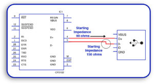
2. Controlled Impedance Routing
- The Impedance should be kept constant at high values for wideband signals to control the parameters of the signal routing. This is especially useful for fast data communication.
- To avoid reflection of signals, don’t forget to set impedance levels accordingly.
- Differential pair routing should be adopted for critical signals, including USB, HDMI, and high-speed data lines.
- To lessen the loss of signal, avoid elongation of signal traces.
3. Vias Design and Positioning
- Vias are critical in the design of HDI PCBs for high-speed circuits. To reduce signal disturbance, use micro vias, blind vias, and buried vias.
- Microvias can be used to cut back on the loss of signals as well as impedance discontinuities.
- Do not use vias on the paths of high-speed signals in order to reduce reflections.
- Utilize via-in-pad techniques for better electrical performance and space performance.
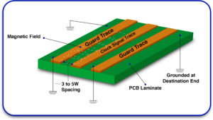
4. Noise and Crosstalk Reduction
Crosstalk is the interfering of adjacent signals through traces which can lead to data being corrupted. To reduce the impact of crosstalk:
- Ensure there is enough space in between the traces.
- Employ ground planes to isolate high-speed signals from interference.
- Use differential pairs in sensitive circuits to maintain the quality of the signal.
5. Proper Power Distribution Network (PDN)
- The integrity of the power is as important as the integrity of a signal. A carefully developed PDN helps guarantee that power is transmitted effortlessly with low noise and minimal voltage distortions.
- Place decoupling capacitors close to the power pins for voltage stabilization.
- Add solid ground planes to lower the resistance return path.
- Minimize inductance by reducing power loop areas.
6. Considerations for Thermal Management
PCBs with high-density interconnects are likely to experience degraded Signal performance because of excess heat inside the device. For thermal issues, one can:
- Use different thermal vias and heat sinks that are compatible to keep the board cool.
- Use materials with high thermal conductivity.
- Design PCBs with even copper distribution to avoid having hot spots.
Learn About: HDI Board Standards for High-Density PCB Applications
Optimizing Signal Integrity Using Advanced Techniques
1. Using Differential Pairs
- In high-speed systems, differential signaling is used for its ability to suppress noise and enhance reliability.
- Trace spacing must be maintained to be uniform to avoid any imbalance in the signal.
- Differential pairs should be routed in parallel and with a minimum length difference.
- The return path should be continuous to avoid distortion of the signal.
2. Design of High-Speed Serial Interfaces
- Like other HDI PCB designs, high-speed interfaces such as PCIe, USB 3.0, and DDR memory require special design considerations.
- Synchronize arrival times by using length matching.
- Use ground isolation between noisy and sensitive circuits for noise separation.
- High-speed signals should be routed on low-spec impedance controlled for a specific layer.
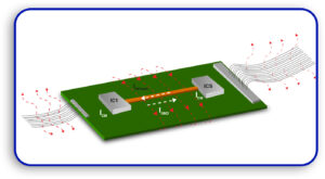
3. Filtering and Shielding for EMI
To shield signals from external noise:
- Use ground planes and shielding enclosures for components that are sensitive to noise.
- Add filtering capacitors at critical nodes of the signal.
- Minimize exposure to EMI using preferred routing techniques for PCB traces.
Best Practices for Companies That Manufacture PCBs
A PCB manufacturing company is guaranteed performance beyond normal expectations of an HDI PCB if it follows the provided guidelines. This includes:
Conducting integrity simulations pre-layout in order to be able to simulate all possible problem areas.
Employing low-loss dielectric materials for PCBs.
Creating prototypes and testing them to validate the signal performance.
Working with qualified manufacturers of PCB boards to improve the processes of PCB fabrication and assembly.
Conclusion:
As explained in IEEE 803.2, HDI PCBs provide the means of realizing advanced modern electronics, but maintaining the precision of signal integrity within the design requires a lot of work. With the implementation of composite materials in controlled impedance routing, advanced via placement strategies, efficient power distribution, and crosstalk minimization, an engineer can make a competitive HDI PCB design. For companies that want to create excellent PCBs with great signal integrity, it is best to work together with a qualified PCB manufacturing company. Blind Buried Circuits focuses on the provision of high-quality printed circuit board design, fabrication, and assembly. Get in touch with us today, and we will equip you with modern tools to design and enhance your HI PCBs for advanced electronics!


