With the development of wireless communication technology, the need for accurate RF PCB design has increased drastically. Designing RF boards in telecommunication, aerospace, automotive, radar, and medicine requires an understanding of engineering principles to ensure minimum signal degradation, interference, and maximum performance. To achieve that, designers need to closely cooperate with fast PCB manufacturers that deal with specialized high-frequency PCB assembly and manufacturing.
This article will examine the essential factors influencing RF design on the PCB, ranging from material selection to the shape and construction of the PCB.
Know More About RF PCB Design
Any design that involves RF PCB is outside the domain of standard PCBs because RF PCB involves the use of signals having frequencies over a range of 100MHZ to 100GHz. Some examples of the applications that utilize these boards are:
- 5G network and wireless communication system
- Satellite and radar systems
- Medical equipment like imaging and RF diagnostic equipment
- IoT and RFID
Since RF signals are more prone to noise, signal loss, and impedance mismatches than other signals, the design of RF boards has to be done extremely carefully in order to minimize signal degradation.
Considerations for PCB RF Design
1. The Importance of Selecting the Right PCB Material
The selected PCB material significantly affects how RF operates. While a regular FR-4 may not possess the most optimal signal integrity for high frequencies, RF PCBs need specially designed laminates with low dielectric loss and excellent electrical properties constancy.
Preferred PCB Materials For RF Design:
- Rogers RO4000 Series: Provides low loss and excellent signal performance.
- Taconic RF Laminates: Known for providing stability at high frequencies and low moisture absorption.
- PTFE (Teflon) Substrates: Most suitable in microwave and millimeter-wave devices.
While RF-friendly materials are needed, they should be available in bulk so that quick PCB manufacturing can take place.
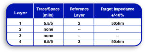
2. Matching of Impedance And Controlled Dielectric Constant
An impedance mismatch always leads to signal reflections, which significantly decreases the performance of an RF PCB, particularly its design. To help avoid such concerns:
- Use controlled impedance stack-ups: Traces must have constant impedance to avoid signal loss.
- Stable dielectric constant (Dk): Material features should not vary to allow for predictable signal behavior.
- Return loss minimization: Proper transmission line techniques, such as micro-type and stripline techniques, need to be employed. These techniques significantly improve signal integrity.
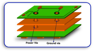
3. Stacked Layer Configuration
To maintain signal fidelity, RF PCBs need interference-free, well-organized layer stack-ups. Recommended RF PCB Stack-Up Instructions: Utilize dedicated ground planes to guarantee a low-impedance path for signals. Separate signal from power layers to avoid interference and cross-talk. Optimize the width and space of traces to aid in the control of impedance. Engaging a PCB manufacturing and assembly services expert ensures that your stack-up meets the design requirements for high frequencies.
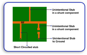
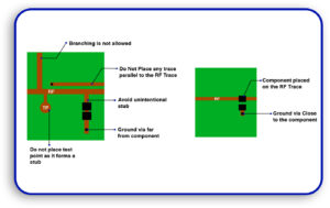
4. Optimization of layout and routing of RF Traces
The RF signal paths have to be short and direct. This will minimize signal degradation as much as possible.
Common RF Trace Routing Mistakes:
- Replace sharp angles with curved traces – Minimizes signal reflection.
- Keep trace widths constant – Allows for impedance matching.
- Segregate RF and digital circuits – Prevents interference.
- Use coplanar waveguides – Improves the integrity of the signal in high-frequency designs.
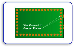
5. Grounding and Shield Techniques
Correct default and ground configurations are pivotal in combining RF characteristics and PCBs. Poor grounding results in cross-talk and noise with the RF signal. Sound strategies for RF shields include:
- Use via stitching: A grid of vias that surrounds the RF trace helps contain EMI (Electromagnetic Interference).
- Shield with metal cans: Physically isolate RF sections from the rest of the PCB.
- Use ground planes: Provide RF signals with a solid return path.
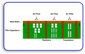
6. Also consider heat management
The heat from high-frequency components can also affect RF performance. Effective heat dissipation ensures stable signal performance.
Dissipation techniques:
- Employ thermal vias to move the heat away from RF components.
- Optimize copper pour distribution to help reduce excess heat.
- Choose low thermal resistivity materials for better heat management.
7. Component Placement and the Isolation of RF Signals
RF circuits are very reactive to noise from surrounding components and circuits. Meticulous placement is required to avoid coupling.
Recommended Component Placement Practices:
- Isolate RF components from digital circuits to reduce signal distortion.
- Place antennas and matching networks in close proximity to minimize transmission losses.
- Utilize power supply isolation to prevent noise coupling.
Working with an RF board PCB manufacturer guarantees that placement and routing will adhere to industry best practices.
8. Validation and Testing of RF PCBs
For the performance of RF PCB, appropriate testing systems must be built to coordinate with rich testing procedures.
General Testing Methods for RF PCBs:
- Vector Network Analysis (VNA): Measures impedance and signal reflection, useful for RF PCB testing.
- Time-Domain Reflectometry (TDR): Monitors signals for discontinuities and impedance mismatches.
- Antenna Performance Testing: Verifies the signal reception and transmission.
Maintaining quality control is a crucial consideration in the manufacture and assembly of the PCB for RF applications to ensure constancy and dependability.
Selecting the Most Appropriate PCB Manufacturing Partner
The design of RF PCB is very intricate and requires design collaboration with a dependable PCB board manufacturer with specialisation in high-frequency applications. While selecting a fast PCB fabrication partner, look at the following:
- Expertise in the fabrication of RF boards – Guarantees precise fabrication of circuits of high frequencies.
- Sophisticated manufacturing technology – Capability to handle tiny pitch components with controlled impedance.
- Defect-free RF performance – Assurance and testing protocols.
- Collaboration with the leaders in flexible PCB fabrication will enable engineers to realize the stringent requirements regarding the quality of the RF PCB design.
The construction of an effective PCB for RF applications should thoughtfully consider the right combination of materials, impedance management, thermal management, and signal integrity, among other things. Through layout optimization, shielding, and testing, engineers can design RF boards that can function reliably in high-frequency environments.
Seeking professional help for your RF PCB fabrication and assembly? Blind Buried Circuits offers high-frequency PCB fabrication services customized according to your requirements. Don’t hesitate to reach out to us today and let us know what your RF board design needs are and enjoy fast PCB manufacturing services with seamless integration!


