There are distinct printed circuit boards (PCBs) wired for ultra-high speeds and currents, and they’re tough to make because of the minute details that need consideration for the material used for the trace layout and connectors. Whether you are dealing with a custom PCB design supplier or doing it yourself, the board needs to be perfectly balanced between loss and performance. Find out how below.
Why Effective Trace Layout is Important
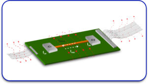
Attention is given to both the high-speed and ultra-high-current designs to ensure the integrity of information transmission and the performance of the printed circuit board (PCB).
The aforementioned factors, including trace width, impedance, and thermal management, are regions that need proper micromanagement.
High Speed and High Current PCB Trace Layout Tips
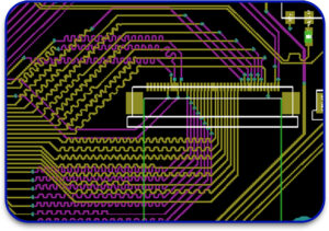
Printed circuit board (PCB) designs that incorporate an element of high speed and high current are not easy and require a careful selection of traces, layout, materials, and connectors. Whether you are working with a custom PCB manufacturing company or doing the design work yourself, optimizing trace layout is very important for reliable operation and the increasing complexity of modern electronic systems.
Knowing how to properly calculate PCB trace widths, handle thermal issues, and choose appropriate high-current PCB connectors dramatically improves overall performance.
Essential Aspects in Creating High-Speed Signal Paths
High-speed signal paths must be free of impedance, mismatches, signal reflection, and all types of noise. The design must consider all of these aspects to maintain the signal’s integrity and functionality.
Maximum Length Rule
The trace length must always be shorter than the critical length (lc), which is defined by the equation Where c is the speed of light in the given medium and f is the signal’s frequency. The trace length lower than lc ensures minimal distortion of the signal.
3 dB Bandwidth: Preventing Signal Loss
A high-speed signal needs bandwidth that allows higher frequencies to pass without attenuation. The 3 dB bandwidth of the trace needs to match the signal to ensure its integrity.
5 Quick Tips To Improve The Design of Traces that Need Higher Speeds
1. Use a Moving Ethnic Serpent for Route Length Pace Making
Serpentine routing allows for the bending of tracks to equalize trace lengths, which helps to ensure that signals arrive at the destination at the same time.
8 Suggestions On How To Design Best Serpentine Traces Longer than 90 Degrees:
– Retain the same width for the trace.
– Do not overdo cuts.
– Maintain constant spacing between loops.
– Use controlled impedance if possible.
– Do not loop over each other as this will increase crosstalk.
– Equal number of loops at the top and bottom.
– Do not add too many turns.
– Use time delay simulation to make the turns.
2. Use Guard Traces to Assist in Reducing Electromagnetic Interference
Guard traces help isolate adjacent traces that are exposed to high-speed signals and electromagnetic interference from other traces.
6 Directions To Apply Guard Traces
– Include guard traces to the ground.
– Ensure constant separation between the signal and guard traces.
– Provide continuous guard traces.
– Ensure guard traces are sufficiently large to offer adequate shielding.
– Use vias at the guard traces to the ground plane.
– Check the effectiveness of the guard traces in the test.
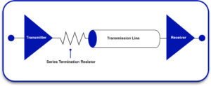
3. Traces Termination to Cease Reflection of the Signal
Termination of traces helps in the prevention of reflection, which can adversely affect signal quality.
Series Trace Termination:
Integrate a resistor in series adjacent to the signal source for proper trace impedance matching.
Parallel/Shunt Trace Termination:
To eliminate signal reflections, a termination resistor should be placed in parallel with the trace to ground or to the DC power supply voltage.
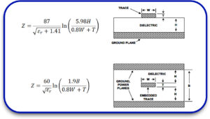
4. Adjust the Trace Shape to Control the Impedance Value
As a rule of thumb, having a specific shape and dimension for the trace guarantees a controlled impedance, which is essential for rapid transmission signals.
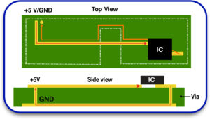
5.Never Split Ground Planes
The splitting of ground planes creates discontinuities in impedance and increases the vegetative index of electromagnetic interference.
6 Best Grounding Practices to Ensure Signal Integrity and Minimize EMI:
- Use a ground layer without cuts.
- Make return paths as brief as possible.
- Prevent ground loops.
- Put vias close to the components to be grounded.
- Provide decoupling capacitance.
- ncrease the spacing between signal traces and the ground plane.
5 High-Current Trace Design Techniques to Ensure Power Integrity
- Determine the Maximum Current that The Trace Can Carr
To get high-current traces, cutouts and edges can be designed using online tools provided by PCB manufacturers. The calculation for traces can also follow the IPC-2221 formula. - Use Wider Traces
Resistance and heating are two significant causes of unreliable current, which can be removed by placing wider traces as more current can be captured. - Place Thermal Vias Near Hotspots
Vias allow heat conduction between layers, and utilizing them in spots with high-temperature reach prevents zone overheating. - Position Decoupling Capacitors Close to the Power Supply Unit
Decoupling capacitors provide voltage regulation and noise suppression in high-power circuits. - Maximize Via Current Carrying Capacity
Using multiple vias in parallel improves current-carrying capacity as well as thermal management.
5 Best DFM Rules for High Speed and High Current PCB Traces
1. Do Not Deviate from the Manufacturer Stipulated Minimum and Maximum Line Widths
Get in touch with your custom PCB fabricator regarding their capability limits.
2. Provide Adequate Trace Separation Depending on the Initial Copper Thickness
It’s essential for spacing to be ample in order to avoid shorts and enhance dependability.
3. Provide At Least 7 Mils of Trace to Board Edge Spacing for Outer Layers and 10 Mils for Inner Layers
This will help to mitigate damage risks during production and walking over the board during handling.
4. Provide a Minimum of 15 Mils from the Edge of any Copper Feature to the V-Score Line
Maintaining proper clearance prevents challenges in separating panels during individual board separation.
5. Set a Minimum of 8 Mils from Any Drill Hole to Copper To Reduce Risk Of Short Circuits
This measure will guarantee reliable electrical separation and lessen the potential for defects in the manufacturing processes.
Best Practices in Case of Collaboration with PCB Board Fabricators
- Early Engagement: Contact your custom PCB board manufacturer during the design phase for more information on capability and constraints to aid the manufacturing process.
- Utilize Design Verification Aid: Embrace design verification tools for performing thermal simulation, impedance matching, and current flow distribution.
- Quality Assurance: Look for manufacturers who have strong quality control measures in place, such as AOI and functional testing.
File Formats for PCB Designs:
The file format used most widely across industries is Gerber files, which store the information for each layer of a PCB.
Other formats could be Excellon for drilling information and ODB++ for detailed manufacturing information.
Creating high-speed and high-current PCB traces requires considerations of signal integrity, heat dissipation, and power delivery. Following best practices such as serpentine routing, guard traces, and proper termination will allow engineers to meet all application requirements. Also, working with a skilled custom PCB manufacturer allows maximum design for manufacturability and design for performance optimization.
Are you ready to enhance your PCB design for advanced performance? Contact Blind Buried Circuits today for customized solutions for your specific design challenges.


