Printed Circuit Boards (PCBs) are the foundation of modern electronics. Whether you are designing a simple circuit or a high-performance system, following the right PCB design guidelines is crucial for efficient manufacturing and long-term reliability. If you work with PCB manufacturing and assembly experts, you know that small mistakes in PCB layout can lead to electrical failures, overheating, or even complete product failure. A well-optimized PCB fabrication process ensures smooth signal transmission, durability, and cost savings.
This blog will discuss the best practices for PCB design, from component placement to trace routing, and how to work effectively with PCB fabrication USA specialists.
Why PCB Design Matters?
A well-designed PCB can improve your product’s performance and reduce production costs. Here’s why optimized PCB design is essential:
1. Prevents Electrical Issues
A poor PCB layout can cause signal interference, electromagnetic noise, and short circuits. By following design best practices, you ensure that signals move smoothly without disruptions.
2. Improves Manufacturability
Working with PCB manufacturing and assembly providers becomes easier when your design follows industry standards. A clean PCB layout reduces errors and speeds up production.
3. Increases Reliability
A good PCB design ensures that components are well-placed, heat is managed effectively, and traces are routed properly. This improves the board’s lifespan and performance.
4. Reduces Costs
Poor PCB design can lead to expensive rework, additional layers, or failed prototypes. Optimized PCB fabrication saves money and time.
Key PCB Design Guidelines for Maximum Efficiency
1. Choose the Right PCB Type
Different applications require different types of PCBs. Choosing the right type ensures better performance and cost-effectiveness.
- Rigid PCBs: Common for consumer electronics and industrial applications.
- Flexible PCB fabrication: Used for wearables, medical devices, and automotive applications due to their flexibility and durability.
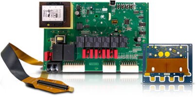
- Rigid-Flex PCBs: Combine rigid and flexible features, ideal for compact and high-performance designs.
Understanding the differences helps you work efficiently with PCB fabrication USA providers to get the best results.
2. Optimize Component Placement
Proper component placement is key to a reliable PCB layout. Follow these rules:
- Group related components together to reduce trace lengths.
- Place high-speed components close to each other to minimize signal loss.
- Keep power components separate from sensitive analog circuits to reduce interference.
- Ensure enough space between components for easy soldering and heat dissipation.
- By placing components strategically, you improve both performance and PCB manufacturing and assembly efficiency.
3. Maintain Proper Trace Width and Spacing
PCB traces carry electrical signals, so their width and spacing affect signal integrity and current flow.
- High-current traces need wider paths to prevent overheating.
- Signal traces should follow a consistent width to maintain signal quality.
- Spacing between traces prevents short circuits and crosstalk.
Using the right trace width helps avoid failures and makes PCB fabrication easier.
4. Implement Proper Grounding Techniques
A strong ground connection is crucial for a stable PCB layout. Follow these best practices:
- Use a solid ground plane to reduce noise.
- Minimize ground loops to prevent interference.
- Use multiple ground vias for multi-layer PCBs.
Proper grounding ensures better electrical performance and prevents noise-related issues.
5. Manage Heat Dissipation
Overheating can damage components and shorten PCB lifespan. Use these strategies:
- Place heat-generating components near edges for better airflow.
- Use thermal vias to dissipate heat.
- Choose high-quality PCB materials with good thermal conductivity.
Good thermal management ensures your PCB lasts longer and works reliably.
6. Use the Right Via Types
Vias connect different PCB layers. Choosing the right type improves both performance and PCB fabrication USA efficiency.
- Through-hole vias: Connect all layers, common in traditional PCBs.
- Blind vias: Connect outer layers to inner layers, used in high-density designs.
- Buried vias: Connect inner layers without reaching outer layers.
- Microvias: Small vias used in flexible PCB fabrication and HDI designs.
Each via type has advantages, so choosing the right one improves PCB manufacturing and assembly efficiency.
7. Follow Industry Standards
Industry standards ensure quality, safety, and reliability. Some key standards include:
- IPC-2221: General PCB design standard.
- IPC-6012: Rigid PCB qualification.
- IPC-6013: Flexible PCB fabrication standard.
- ISO 9001 & ISO 13485: Medical device PCB quality control.
Working with a PCB fabrication USA provider who follows these standards ensures you get a high-quality product.
Common PCB Design Mistakes to Avoid
Even small mistakes in PCB layout can lead to big problems. Here are some common issues to avoid:
1. Insufficient Trace Clearance
If traces are too close, they can cause short circuits or crosstalk. Always follow minimum clearance guidelines.
2. Poor Component Placement
Crowded components can lead to poor soldering, overheating, and difficult assembly. Leave enough space for proper airflow and connections.
3. Not Accounting for Manufacturing Constraints
Ignoring fabrication limitations can lead to production delays. Always check with your PCB manufacturing and assembly partner before finalizing the design.
4. Skipping DFM (Design for Manufacturability) Checks
DFM checks ensure that your PCB can be manufactured without errors. Work with a PCB fabrication expert to review your design before production.
How to Work with a PCB Manufacturer for Best Results
1. Choose an Experienced Manufacturer
Select a PCB board manufacturer with experience in your industry. If you need flexible PCB fabrication, work with specialists in flex circuits.
2. Communicate Design Requirements Clearly
Provide detailed Gerber files, layer stack-up information, and material specifications to ensure accurate manufacturing.
3. Request a Prototype Before Full Production
A prototype helps you identify design flaws before mass production. Many PCB fabrication USA companies offer quick prototyping services.
4. Conduct Quality Testing
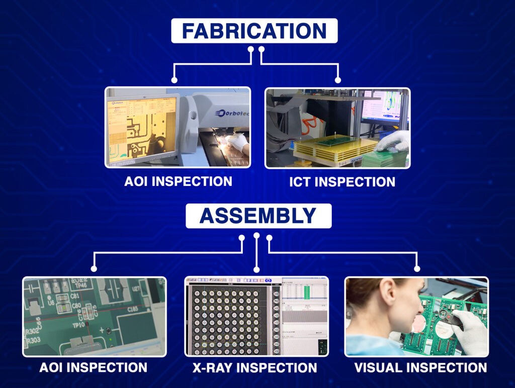
Always perform electrical testing, thermal analysis, and stress testing to ensure your PCB meets design requirements.
Future Trends in PCB Design
1. AI-Assisted PCB Design
Artificial intelligence is making PCB layout optimization faster and more accurate, reducing design errors.
2. Advanced Flexible PCBs
With the rise of wearable devices and medical electronics, flexible PCB fabrication is becoming more common.
3. Higher Density and Miniaturization
As devices shrink, high-density interconnect (HDI) technology will play a bigger role in PCB manufacturing.
4. Environmentally Friendly PCB Materials
Manufacturers are shifting toward lead-free and recyclable PCB materials to reduce environmental impact.
A well-designed PCB layout ensures efficiency, reliability, and cost-effectiveness. By following these essential guidelines, you can prevent common design mistakes and work smoothly with PCB manufacturing and assembly partners. Whether you are working with a PCB fabrication USA provider or designing flexible PCB fabrication, optimizing your design from the start will save time and money.
Would you like expert advice on your PCB project? Contact an experienced PCB board manufacturer today to ensure your design meets industry standards and performs at its best.


