The ever-growing demands of the contemporary electronics sector require that printed circuit boards (PCBs) be of a higher design complexity while also being miniature to properly fit within sophisticated systems ranging from telecom and aerospace to medical equipment. Microvia technology, for example, is an essential step in this evolution.
If properly engineered and executed, microvias will greatly improve a PCB’s capability and strength, especially in the case of HDI board circuits. Every PCB board vendor needs to be well versed in the design principles of micro vias in order to produce adequately complex boards that satisfy client specifications. Let us look at some factors that make micro via PCB design so important in the fast-paced world of modern electronics.
What Are Microvias?
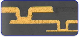
Microvias are interconnected holes or vias within the PCB used to manage side-to-side connections on different board layers. Their diameters do not exceed 150 microns, making them significantly smaller than standard vias. These features are of extreme importance in HDI board circuits since they provide higher routing density and superior electrical performance.
Microvias are classified based on their locations and purposes:
- Blind Microvias: These are used to connect an outer layer to one or more inner layers. However, they do not go all the way through the board.
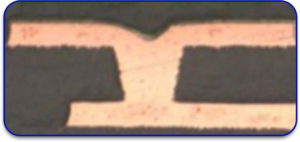
- Buried Microvias: These are embedded completely within the internal layers which makes them hidden from the surface.

- Stacked and Staggered Microvias: Incorporates complex designs better suited for space optimization and performance enhancement.
Benefits of Microvia Technology
Microvias have a number of merits when compared to conventional vias, which render them essential in most PCB manufacturing and assembling processes:
- Higher Component Density: Microvias increase the density of components on the PCB by requiring minimal space for interconnections.
- Enhanced Signal Integrity: Reduced interconnection spacing of PCB lowers the signal loss, noise, and delays experienced by the circuit.
- Improved Heat Dissipation: Good thermal management increases the performance and durability of the board.
- Compact and Lightweight Designs: This is best suited for portable applications and devices that operate under space constraints, such as wearables and aerospace electronics.
- Reliable Performance: Microvias lead to more reliable PCB structures that can endure high magnitudes of mechanical stress.
Design Essentials for Microvia PCBs
1. Material Selection
The materials used in micro via PCBs must be chosen carefully in order for them to function as intended. They must also have the required thermal stability, dielectric constant, and mechanical strength.
Best Practices:
Employ high-Tg (glass transition temperature) laminates to allow for thermal cycling.
Opt for copper foils with lower surface roughness to enhance most signals.
Ensure compatibility with means for accurately creating microvias, such as laser drilling.
2. Microvia Positioning
The positioning of microvias should be strategically selected for maximum optimization of the PCB performance parameters and durability.
Guidelines For Placement:
To lessen mechanical damage, do not place microvias too close to each other.
Place microvias next to heat-producing components to allow for optimal heat removal.
Placement should be done with symmetry to ensure structural integrity.
3. New Techniques in Copper Microvia Drilling
Microvias should be made using laser drilling as it is the most precise and allows the production of holes through thin layers.
Benefits of Laser Drilling:
Everything is highly precise, including the measurement of the drill hole.
Materials surrounding the hole do not get damaged easily.
Drilling is done more effectively and is easier than using a mechanical drill.
4. Other Techniques Used in Electroforming Microvias Copper Plating Includes Filling and Drilling
Drilling, plating, and filling micro vias should be done appropriately to ensure that electrical connections are reliable and have great mechanical stability.
Methods:
Copper electroplating should be done to achieve uniform thickness for the micro via.
Filling the via with conductive and, in some cases, non-conductive materials should strengthen the micro via’s thermal and mechanical strength.
5. Stacked Microvias Design Structure
Microvia design requirements make layered structure stack-up design highly important.
What Needs to be Considered:
A balanced stack-up to preserve structural integrity must be used.
The core of the board should provide better signal integrity through the power and ground layers being redistributed.
Stacked micro vias with staggered placements can be used to meet the design requirements of more complex structures.
6. Evaluation And Validation Of Design Microvia Pcb
In the modern approach, microvia PCBs are tested and verified for performance and reliability to ensure standards are met.
Approach For Testing:
Electrical continuity tests should be done for verification of connections.
Thermal cycling should be done to test robustness.
Using X-Rays to Find Defects.
Microvia PCBs Applications:
Microvia technology is adopted widely because it improves the functionality and reliability of the PCB in every industry.
- Consumer Electronics: Microvia PCBs are required for the compact and light designs of smartphones, tablets, and wearables.
- Aerospace and Defense: Microvia HDI board circuits work more reliably in worst-case scenarios.
- Medical Devices: Complex medical equipment requires the strongest and densest PCBs.
- Automotive Electronics: ADAS and infotainment systems rely on microvia PCBs.
Microvia Technology Reliability and Failure Prevention
No question that keeping microvia PCBs reliably in a system damage performance is paramount. These include cracks, voids, and delamination.
How to Enhance Reliability:
- Establish robust design rules and run simulations at the design stage.
- Select good quality materials and accurate processes during manufacture.
- Test and inspect many aspects of the product.
- Use an experienced provider of PCB manufacturing and assembly services.
Developments in Microvia PCB Technology
Microvia technology is constantly evolving, and these developments include:
- Laser Direct Imaging (LDI) – allows microvias to be patterned more accurately.
- Embedded Components – placement of components inside the PCB layers for space and performance improvement.
Improved copper plating methods that enhance overall conductivity and reliability. Smart PCB Designs Incorporate sensors and monitoring features.
Why Blind Buried Circuits the Best for Microvia PCBs?
We at Blind Buried Circuits have years of experience delivering quality PCB manufacturing and assembly services designed to meet today’s standards. As a revered micro via PCBs manufacturer, we deploy sophisticated manufacturing technology and methods to deliver micro via PCBs for a range of industrial applications.
What We Offer:
- High competency in HDI board circuits and microvia technology.
- Custom offerings based on your business needs.
- Advanced manufacturing techniques and comprehensive quality assurance.
Would you like to make your next project stand out using innovative micro via PCBs? Contact us and start the journey to your next innovation with us today.


I simply could not depart your website before suggesting that I actually enjoyed the standard info an individual supply in your guests? Is going to be again continuously in order to check up on new posts