PCBs are at the heart of all gadgets, from consumer electronics to industrial machinery. Nevertheless, one of the common problems that may result in failures and expensive repairs is PCB delamination, which is essentially a malfunction for the reason that different layers of a PCB separate. This can lead to electrical failures, lower performance, and a shorter lifespan of the board.
To custom PCB production or perform fast PCB manufacturing, maintenance of durability over time is very important. In this tech tip, we’ll outline reasons for PCB delamination, offer ways to stop it, and explain ways to extend the life of PCBs.
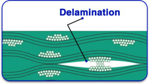
What Is PCB Delamination?
Delamination of PCBs occurs when the layers of it begin to separate because of insufficient bonding between them and the materials making components of a PCB. This results in bubbles or voids forming between these layers which causes issues like signal disruption, conductivity failure, and weakness in structure. Building up PCBs requires stacking several layers of copper, insulating material, and adhesives, so they require good bonding. Preclusion is the most effective means possible because once the damage caused by delamination happens, there is no way to turn back.
Why Does PCB Delamination Occur?
Delamination occurs due to many factors and most of them relate to poor material choice, faulty manufacturing processes, or forms of environmental strain. Following is some of the underlying reasons:
1. High Moisture and Heat
Soldering, operation, or environmental conditions all expose PCBs to elevated heat levels. If the board is poorly constructed to manage heat, parts tend to expand at differing rates, thus causing separation. Additional humidity causes the glue to weaken, which results in delamination.
2. Unfavorable Material Choice
Low-quality laminates that are not able to endure elevated temperatures or mechanical strain are highly likely to lead to delamination. They are also not able to withstand high-quality thermosetting resins. Poor choice of prepreg (insulating material between layers) can lead the PCB structure to become weaker.
3. Faulty Lamination Technique
PCBs are constructed with multiple layers that need to be thermally activated, which means they are bonded with the application of heat and pressure. Under lamination, a step is done to bond previously activated layers together, some air gets trapped, and adhesion becomes weaker, leading to delamination.
4. Bending And Mechanical Strain
Bending and twisting or any movement that is deemed excessive can form micro-cracks through PCB layers, which eventually lead to separation. This is prevalent in flexible printed circuit boards that require extra support and reinforcement.
5. Chemical Contamination
The adhesive bonding between layers may be affected by chemical residues of etching or plating and soldering. If the PCB is not adequately cleaned, pollutants may cause delamination over time.
Methods to Prevent PCB Delamination
Delamination of PCB involves good design decisions, first-rate materials, and precise controls during manufacturing. Below are the key pointers to guarantee PCB durability for an extended period:
1. Use Advanced Materials for PCB Fabrication
The materials you choose for the fabrication also aid in the prevention of delamination. This is what to search for:
- Materials with Advanced Glass Transition Temperature: High-Tg laminates (above 170°C) are easier to expand and can withstand heat better.
- Low Moisture Loss Materials: Laminates with low moisture loss, such as FR-4 High Tg, Polyimide, or PTFE, aid in preventing delamination due to humidity.
- Increased Copper to Substrate Bonds: Withstanding the copper layer and the substrate improves durability over a long period.
2. Manage Heat Exposure
As the fast manufacture of PCBs involves several processes that require high temperatures, the control of the heat is of concern:
- Employ thermal reliefs and vias.
- Do not allow too many reflow cycles for soldering.
- Increase and decrease the temperatures of the PCBs slowly to avoid thermal shock.
- PCBs should be kept in a dry place before soldering so as to avoid moisture.
3. Enhance the Lamination Process
A well-managed lamination always prevents the splitting of layers:
- Correct pressure and temperature must be applied during the lamination.
- A multi-stage curing cycle must be used to strengthen adhesive bonds.
- Bonds need sufficient curing time to ensure all air and moisture that might cause weak bonding is removed.
4. Mechanical Strain Should Be Minimised
External and operational assembly can result in mechanical damage impact that affects PCB layers:
- Appropriate handling implements should be used to avoid flexing and bending.
- Incorporate features into boards that enable flexible areas to be reinforced for relief of stress.
- Use stiffeners to increase support for flex PCBs.
5. Ensure That PCBs Are Free From Dirt
Obstructions hinder bonding from taking place, leading to delamination. To avoid this:
- During the etching and plating processes, high-purity chemicals should be used.
- After chemical processes, PCBs should be rinsed and dried properly.
- Prior to lamination, an inspection of cleanliness has to be conducted to remove any external particles.
6. Conduct Reliability Testing
To enhance PCB endurance, manufacturers should execute:
- Cross sectional peel strength assessment to check for bonding gaps.
- Thermal shock tests imitate changes in temperature and humidity.
- Moisture damage test to check PCBs’ ability to withstand failure due to moisture.
Inspection and Testing Measures Against Delamination
If undetected, these delamination problems can lead to catastrophic failures. A good inspection of a circuit board shall include:
1. X-ray and Polygraph Inspection
- AOI (Automated Optical Inspection) discovers surface anomalies prior to assembling the unit.
- X-ray images show internal delamination of the multilayer circuit boards.
2. Microsection Analysis
The Microsectioning process of AC-titled stick PCB prepares it for examination of layer bonding to look for gaps, voids, or weak adhesion.
3. Thermal Stress Testing
PCB design for extreme conditions is tested under delamination simulation conditions for the scope of survival in real-world extreme temperature and humidity conditions.
Achievable Goals with Enduring PCBs
Delamination of PCBs is a critical problem, but it can be resolved by these processes of using quality materials, effective manufacturing, and adequate testing. Custom PCB production, fabrication or quick turn PCB fabrication are equally supported with the listed practices, making the boards long lasting, reliable, and strong. Blind Buried Circuits specializes in fast PCB manufacturing. Our PCBs are fabricated and assembled with technology guaranteeing the absence of delamination while providing high-quality exploitation characteristics.
Do you seek a reliable supplier for PCBs? Get in touch with Blind Buried Circuits and get the professional help required for the sustainability of your PCB boards.


