Microvias are critical features on printed circuit boards (PCBs) and in High-Density Interconnect (HDI) designs. These minute sites assist in associated interlayer connections in intricate PCBs.
This feature makes it possible to optimize the given space and improve the performance of electronic circuits. But for microvia geometry to be effective, appropriate reliability assessment is needed for given nominal performance and expected life.
Furthermore, this guide will emphasize the significance of HDI microvia reliability, suggest various remedies to prevent failures during fabrication processes, and discuss ways to collaborate with PCB board manufacturers to accomplish favorable outcomes.
Designing Microvia for Reliability Issues
Microvias are defined as drilled holes that connect layers in a PCB using a laser. They are dominant in most HDI designs because of high premiums on precision and space. Reliable microvia design ensures that these connections withstand the thermal and mechanical stresses associated with PCB assembly and manufacturing processes.
Still, microvia roughness or out-of-focus vignetting can result in considerable performance issues or even lead to board destruction. Multiple laminate cycles, combined with elevated temperatures and expansion of materials, jeopardize the microvias’ integrity. These loosely exposed elements require attention for PCBs to maintain better reliability and robustness.
Common Causes of Microvia Failure
1.High-Temperature Dielectric Materials
With the switch from traditional tin-lead solders to high-thin alloys, PCBs are now subjected to higher operational temperatures during reflow processes. This increase introduces greater thermal stress to copper interconnections and base materials, often resulting in HDI microvia failure.
2. Expansion Rate Mismatch
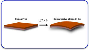
PCB materials, like copper and glass epoxy, expand at different rates during thermal cycles. Copper expands at 16 parts per million (ppm), while glass can expand up to 200 ppm. This mismatch creates strain, leading to cracks or separation at the microvia interfaces.
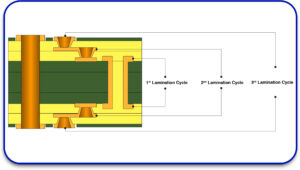
3. Multiple Lamination Cycles
HDI microvia designs may require multiple lamination cycles. Residual thermal cycles and pressure from repeated lamination processes can cause extreme damage to plated holes in the long run.
Reliable Microvia Design Tips
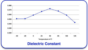
1. Select Appropriate Dielectric Material – Materials such as Isola FR408HR, FR370HR, I-Speed, and Nelco N7000-2HT ensure reliable microvia creation with high material uniformity. This improves the overall manufacturing process.
2. Comply With IPC-T-50M Standards – Critical microvia design parameters include:
- 1:1 maximum aspect ratio
- Hole diameter up to 6 mils
- Capture pad and target pad distance equal to or lower than 10 mils.
Following these requirements minimizes errors and improves manufacturability.
3. Use Staggered Microvias Instead of Stacked Microvias – Staggered microvias can endure more thermal cycles than stacked ones. Ensure the vertical distance between staggered microvias is larger than the hole diameter to improve thermal management.
4. Optimize Stack-Up Design According to IPC-2226 –Proper stack-up configuration improves manufacturability and heat management. Common configurations include:
- Type I: Contains a plated through hole (PTH) and microvia layer on top.
- Type II: PTH, buried via, and microvia layer.
- Type III: At least two microvia layers on one or both sides of the core in a staggered disposition.
5. Ensure No Space Between Microvia and Solder Mask – The solder mask’s clearance to the microvia should be zero to prevent solder bridging during reflow. This ensures dependable connections.
Microvia Testing for Reliability
Testing microvias is crucial to building confidence in their reliability. Leading PCB manufacturers use test coupons (sprouts from the main PCB) to check workmanship quality.
Microvia Reliability Test Methods
- Method 2.6.27: Tests resistance after six reflow cycles at peak temperatures of 230°C or 260°C.
- Method 2.6.7.2: Includes six reflow cycles and measures thermal shocks (100 cycles) from -55°C to +210°C.
Any deviation beyond 5% is considered a failure.
Essential Elements of a Reliable Microvia Design
- Mitre Usage: Separate microvia holes and the dry film for effective laser ablation and electroless plating.
- Staggered Microvias: These are more reliable than stacked microvias due to their lower thermal expansion coefficient and improved heat management.
- Follow Industry Standards: Adhere to IPC-T-50M and IPC-2226 to eliminate design complications and achieve optimal results.
Partnering with a trusted PCB manufacturer and using strong HDI microvia designs can significantly improve the lifetime and performance of PCBs. Reliable microvias not only enhance performance but also reduce the risk of failure in high-stress environments.
Need expert guidance on your microvia designs? Contact the experts at Blind Buried Circuits and ensure your PCB designs are both dependable and efficient.


