PCBs created for RF applications present some difficulties regarding the via layout. The vias connecting the different layers of a multilayer PCB are important conductive pathways, but when not properly placed, they can also lead to thermal issues, impedance mismatches, and parasitic effects. This means that working with a competent PCB board manufacturer is essential for achieving the desired results.
In this article, the focus will be placed on the practical problems of RF PCB via layout and strategizing ways with which to address them so that engineers can maximize signal integrity, minimize interference, and design solid circuits.
The Relevance of RF PCB Vias and Their Functionality
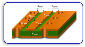
Vias are small plated holes in cylindrical shape that connect different layers of a PCB, enabling vertical transfer of signals or power. In principle, they seem simple, but they play a critical role in the RF performance of PCBs in high-frequency applications (from 1 GHz to 30 GHz).
The common types of vias used in the RF PCB design include
- Through-hole vias: Pass entirely through the PCB; often less ideal for high-frequency circuits due to higher parasitic inductance.
- Blind vias: Connect outer layers to inner layers without going all the way through; reduce signal loss.
- Buried vias: Exist entirely within inner layers; improve space efficiency and signal isolation.
- Stitching vias: Enhance grounding and shielding along RF traces to control EMI and maintain signal iand
Key Challenges in Designing RF PCB Vias
Let’s highlight the key challenges in designing RF PCB vias.
Parasitic Effects.
Vias are introduced within a PCB with parasitic capacitance and inductance, disrupting RF signal transmission. This can lead to signal distortion, reflection, and loss.
Impedance Mismatches
Vias that are poorly spaced out or inadequately designed can cause impedance mismatches, which increase signal reflection while reducing bandwidth.
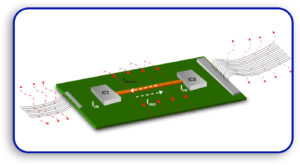
Electromagnetic Interference (EMI)
The signal degradation and noise issues are enhanced by improperly placed via or insufficient grounding planes.
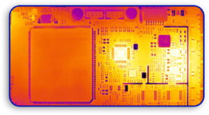
Thermal Issues
Vias can be described as conduits that transfer heat away from components thereby helping in thermal management. Overheating due to poor design can lead to component failure.
To transform these challenges into a possibility, engineers ought to have a solid understanding of RF board design alongside collaborating with reliable PCB board manufacturer.
Guidelines for Touching Issues Related to RF PCB Via
Reduce Via Dimensions
Reducing the diameter of the via from 0.2mm (8 mil) to 0.4mm (16 mil) reduces parasitic inductance.
Why it matters: Smaller diameter vias have less parasitic inductance and better signal integrity.
Implementation Tip: Work with your PCB fabrication company and choose the smallest diameter possible for their fabrication process.
1. Proper Via Separation
The distance between the stitching vias should not be less than λ/20 to limit the impedance mismatch.
Why it matters: Proper spacing allows for less coupling of unwanted signals and consistent signal amplification.
2. Introduce Ground Return Vias
For the frequency lower than 3GHZ, ground return vias should be placed next to the signal vias to maintain impedance.
Why it matters: A ground return provides a return path for the current traveling through the signal, helping reduce EMI while maintaining signal integrity.
3. Employ Via Fencing For High Signals
Signal frequencies above 5GHz benefit from a via fence placed around grounded coplanar waveguides. This enhances isolation and reduces interference.
How Implementing These Strategies Matters: Via fencing helps dampen unwanted frequencies and reduces the chances of other signals being disrupted.
Implementation Tip: To fully enhance the shielding, keep uniform distances between the vias in the fence.
4. Augment Pad and Antipad Measurements
Maintaining an appropriate size for pads and antipodes regulates the via’s impedance and keeps the capacitance level low.
Why It Matters: Capacitance dip and signal reflections are caused by wrongly sized pads and antipods.
Implementation Tip: Employ a variety of tools to adjust the size of the pads and the antipods so that they provide maximum via impedance.
5. Abolish Non-Operational Pads (NOPs)
Non-functional pads can add extra parasitics that are detrimental to the signal’s strength and quality.
Why It Matters: NOPs will increase the ratio of capacitance and can cause a mismatch of impedance.
Implementation Tip: Work together with your PCB fabricator to find and delete excessive NOPs.
6. Employ Back Drilling to Eradicate Via Stubs
By back drilling, you can excise the unused sections of the vias to minimize signal bouncing.
Why it Matters: Via stubs are unneeded and act as antennas whose makers are discontinuous.
Implementation Tip: Work with your PCB board fabricator to maintain uniformity in the back drilling for accuracy.
7. Fill Vias with Conducive Substance
Enhancement of thermal and electrical performance can be achieved by filling the via with copper or conductive epoxy.
Why it Matters: The filled vias increase the structure’s strength, thermal conductivity, and electrical stability.
Implementation Tip: Make sure the manufacturer can supply capped and filled vias.
8. Design Testing and Simulation
Simulation capabilities like HFSS and ADS assist in the optimization of designs by modeling wave propagation.
Importance: The simulator can inform about any conceivable problems during fabrication, leading to cost and time savings.
Tip for Implementation: Create prototype models for high-frequency applications and perform simulations to verify the results.
9. Engage Experienced PCB Fabricators
An expert PCB manufacturer guarantees that proper design rules were adhered to and all constraints were met during fabrication.
Importance: An RF-savvy manufacturer will comment on via design and fabrication in the most valuable manner.
Tip for Implementation: Discuss your design parameters with the PCB manufacturer as early as possible for their input.
Via design on RF PCBs is a crucial process for maintaining the high-frequency signal with the minimum desired interference. Other acceptable practices, such as effective via diameter reduction, maintaining adequate spacing between them, and adequate specialization of PCB board manufacturer, will allow the engineers to solve most of the issues in construction and produce good-quality RF designs.
If you are involved in compiling systems for 5G, IoT, or high-performance radar technology, you should not forget that these techniques will assist you in making better and more reliable PCBs. The effort that should be put into developing the design, simulation, and collaboration with the capable PCB fabricator all aid in achieving successful results.
For such useful information and to witness the services of reliable PCB board manufacturers, visit Blind Buried Circuits.


