Have you ever wondered why some PCBs last longer and perform better than others? One of the key factors is balanced copper distribution. If copper is not evenly spread across a PCB, it can lead to warping, electrical failures, and poor manufacturing outcomes. Whether you are working with Custom PCB production or large-scale PCB production in the USA, achieving the right balance is critical.
As a pcb board manufacturer, understanding copper weight, PCB thieving, and even copper spreading can help prevent design flaws that may affect durability and performance. This blog will guide you through the importance of balanced copper distribution, its impact on PCB reliability, and how you can optimize your design to ensure the best results.
What is Copper Distribution in PCB?
Copper distribution refers to how copper layers are spread throughout a printed circuit board. A well-balanced PCB ensures that copper is evenly placed across all layers, preventing mechanical and electrical issues.
Why is Copper Used in PCBs?
Copper is an essential material in PCB production USA because:
- It conducts electricity efficiently.
- It dissipates heat to prevent overheating.
- It forms a strong connection between components.
However, if copper is not evenly distributed, it can cause etching issues, electrical imbalances, and board deformation.
Why is Balanced Copper Distribution Important?
If copper is not spread evenly in custom PCB production, it can cause serious manufacturing and performance problems. Here’s why:
1. Prevents PCB Warping and Bowing
When copper is unevenly placed, different areas of the board expand at different rates during heating. This causes the PCB to bend or warp, making assembly difficult.
2. Improves Etching Consistency
Uneven copper distribution can result in over-etched or under-etched traces, which affects the PCB’s functionality. A well-balanced PCB ensures that traces maintain their correct width and spacing.
3. Enhances Electrical Performance
Copper distribution directly affects signal integrity. Uneven layers can cause impedance variations, leading to signal loss and EMI (electromagnetic interference).
4. Reduces Manufacturing Defects
Proper copper balance minimizes plating problems, misalignment, and soldering issues during PCB fabrication. This improves the overall quality and yield of production.
5. Better Thermal Management
A balanced PCB spreads heat more evenly, preventing hot spots that can damage sensitive components.
Understanding Copper Weight in PCB Design
Copper weight is measured in ounces per square foot (oz/ft²) and determines the thickness of copper layers. Standard copper weights include:
| Copper Weight | Thickness (Microns) | Usage |
| 0.5 oz/ft² | 17.5 µm | Low-power circuits |
| 1 oz/ft² | 35 µm | Standard PCBs |
| 2 oz/ft² | 70 µm | Power electronics |
| 3+ oz/ft² | 105+ µm | High-current applications |
If one PCB layer has significantly more copper than another, it can lead to mechanical stress and warping during fabrication.
How to Achieve Balanced Copper Distribution in PCBs?
To ensure a well-balanced PCB, pcb board manufacturers use several design techniques.
1. Apply Copper Thieving for Uniform Density
PCB thieving is a technique that adds small copper patterns in areas with low copper density to improve balance. This helps:
- Prevent uneven etching.
- Avoid mechanical stress on the board.
- Improve copper plating uniformity.
However, thieving should be placed carefully away from signal traces to avoid interference.
2. Maintain Even Copper Coverage Across Layers
A common mistake is having one layer heavily loaded with copper while another has very little. This imbalance causes unequal expansion rates, leading to warping. To prevent this:
- Spread copper evenly on all layers.
- Use ground and power planes to balance copper weight.
- Avoid large copper-free areas.
3. Optimize Trace Routing for Better Balance
Traces should be evenly distributed to maintain a consistent copper density. Tips for better routing include:
- Using uniform trace widths.
- Keeping traces spaced evenly.
- Avoiding excessive use of wide traces on one layer while keeping another layer empty.
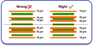
4. Use Symmetrical Layer Stacking
For multilayer PCBs, layers should be symmetrically stacked to maintain mechanical stability. A balanced stack-up includes:
- Evenly placed power and ground planes.
- Matching copper distribution on opposite layers.
- Using identical materials on both sides of the PCB.
5. Ensure Proper Thermal Management
Copper is excellent at conducting heat, but uneven heat distribution can damage components. To improve thermal balance:
- Use thermal vias to transfer heat evenly.
- Spread high-power components across the board.
- Add heat sinks or thermal pads for additional cooling.
Learn About: PCB Thermal Profiling in PCB Assembly
The Role of PCB Thieving in Copper Distribution
PCB thieving is a method used to ensure a more even copper distribution by placing non-functional copper areas in copper-deficient sections.
How Does PCB Thieving Work?
- Identifies low-copper density areas.
- Adds small copper dots or grids to balance the design.
- Prevents etching inconsistencies.
Advantages of PCB Thieving
- Reduces warping and bowing.
- Ensures even etching and plating.
- Improves mechanical stability of the PCB.
Common Mistakes in Copper Distribution and How to Fix Them
Even with the best design practices, some mistakes can lead to copper imbalance. Here are a few errors to watch out for:
1. Uneven Copper Spread Across Layers
Mistake: One side of the PCB has much more copper than the other.
Solution: Always maintain balanced copper coverage on both sides.
2. Large Copper-Free Areas
Mistake: Some regions have too little copper, causing manufacturing defects.
Solution: Use PCB thieving to add small copper patterns.
3. Poor Ground Plane Placement
Mistake: Ground planes are placed randomly, leading to electrical issues.
Solution: Ensure symmetrical ground plane positioning for stability.
4. Ignoring Thermal Expansion Differences
Mistake: Copper expands at a different rate than the PCB substrate, causing cracks.
Solution: Use materials with similar thermal expansion rates.
Achieve a Well-Balanced PCB for Better Performance
Balanced copper distribution is essential for PCB reliability. Whether you’re designing high-speed PCBs, power electronics, or flexible circuits, ensuring even copper placement improves manufacturability and durability.
If you are looking for Custom PCB production with expert guidance on copper distribution and PCB manufacturing, Blind Buried Circuits provides high-quality fabrication solutions. Contact us today to ensure precision and durability in your next PCB project.


