Have you ever wondered how modern PCBs achieve such high-density connections while remaining compact and reliable? Laser drilling technology is a game-changer in advanced PCB fabrication, allowing manufacturers to create highly precise vias for miniaturized and high-performance electronics.
In today’s electronics industry, turnkey PCB manufacturing relies on laser drilling in PCBs to produce faster, more reliable, and high-density circuit boards. Whether it’s for consumer electronics, aerospace, medical devices, or automotive applications, turn key PCB assembly requires cutting-edge PCB drilling processes to meet evolving industry demands. In this article, we’ll break down the importance of laser drilling, how it works, its advantages over mechanical drilling, and its role in high-performance PCB manufacturing.
What is Laser Drilling in PCBs?
Laser drilling is a non-contact, high-precision process that uses focused laser beams to create microvias and through-holes in printed circuit boards. Unlike mechanical drilling, laser technology can drill extremely small, clean, and accurate holes, which are essential for HDI (High-Density Interconnect) PCBs.
Modern turnkey PCB manufacturing requires precisely drilled microvias to connect different PCB layers without compromising signal integrity or board strength. Laser drilling technology is essential for creating these microvias, especially in high-layer-count, compact, and complex PCBs.
Why is Laser Drilling Important?
As electronics become smaller and more powerful, PCBs must be designed with fine-pitch components and high interconnect density. Mechanical drilling struggles with small vias and high layer counts, making laser drilling the preferred method for modern PCB fabrication.
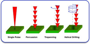
How Does Laser Drilling Work?
Laser drilling in PCB manufacturing assembly works by focusing a high-energy laser beam on the PCB surface to remove material in a precise, controlled manner. The process involves vaporization, melting, and material ejection, ensuring clean and accurate hole formation.
Types of Laser Drilling Technology
There are three main types of lasers used in turnkey PCB manufacturing:
CO₂ Lasers:
- Best for drilling large-diameter holes in organic PCB substrates like FR-4 and polyimide.
- Uses infrared wavelength, which is absorbed by the dielectric material but not by copper.
- Requires a mechanical step to remove excess copper after drilling.
UV (Ultraviolet) Lasers:
- Ideal for fine-pitch microvias due to high precision and low thermal impact.
- Can drill through both dielectric materials and copper layers in a single step.
- Preferred for high-speed, fine-resolution applications like HDI PCBs and flex circuits.
Fiber Lasers:
- Used for metal-based PCBs like aluminum or copper-backed boards.
- Provides high-speed, energy-efficient drilling for power electronics and RF applications.
Each type of laser drilling technology has its specific applications, depending on material type, via size, and production requirements.
Advantages of Laser Drilling Over Mechanical Drilling
Traditional mechanical drilling is limited in precision, speed, and hole size, especially when working with dense and multi-layer PCBs. Laser drilling in PCBs offers several key advantages:
1. Higher Precision and Smaller Vias
- Mechanical drills cannot efficiently produce vias smaller than 150 microns.
- Laser drilling enables microvias as small as 20 microns, perfect for HDI PCBs and fine-pitch BGA components.
2. Non-Contact, Damage-Free Drilling
- Mechanical drilling exerts stress on the PCB, causing delamination or cracks.
- Laser drilling is a non-contact process, reducing mechanical stress and material damage.
3. Faster Drilling Speeds for Mass Production
- A laser drill operates at extremely high speeds, drilling thousands of vias per second.
- Ideal for high-volume production, reducing overall manufacturing time and costs.
4. Enhanced Design Flexibility
- Supports high-density PCB designs with tighter via placements.
- Enables multi-layer interconnections crucial for modern RF, aerospace, and IoT devices.
5. Suitable for a Wide Range of Materials
- Mechanical drills struggle with rigid-flex PCBs, ceramic substrates, and ultra-thin materials.
- Laser drilling technology works efficiently on FR-4, polyimide, PTFE, and high-frequency laminates.
By integrating laser drilling into turnkey PCB manufacturing, manufacturers can produce high-performance, durable, and miniaturized PCBs with superior signal integrity and reliability.
The Role of Laser Drilling in Turnkey PCB Manufacturing:
Turnkey PCB manufacturing involves a complete, streamlined PCB production process, from design and fabrication to assembly and testing. Laser drilling plays a critical role in ensuring quality, efficiency, and advanced design capabilities.
Key Applications of Laser Drilling in PCB Manufacturing:
1. High-Density Interconnect (HDI) PCBs
- Essential for multi-layer, high-speed boards with dense component placement.
- Reduces trace lengths, improving signal performance and thermal management.
2. Rigid-Flex and Flexible PCBs
- Allows precise drilling on thin, flexible substrates without causing material distortion.
- Critical for medical devices, wearables, and aerospace electronics.
3. RF and Microwave PCBs
- Enables the production of high-frequency, low-loss circuits.
- Supports PTFE-based laminates, used in radar and wireless communication systems.
4. Automotive and Aerospace Electronics
- Withstands harsh environments, vibrations, and temperature variations.
- Ensures long-term reliability for mission-critical applications.
5. Medical Electronics and Implantable Devices
- Supports ultra-small PCB designs required for bioelectronics and medical implants.
- Enhances precision and durability in medical applications.
Best Practices for Laser Drilling in PCB Fabrication
To achieve the best results with laser drilling technology, PCB manufacturers must follow optimized fabrication processes:
1. Proper Material Selection
- Use low-outgassing, high-temperature-resistant materials to prevent defects.
- Choose laser-compatible substrates like polyimide, PTFE, and advanced FR-4 laminates.
2. Optimized Via Design
- Use staggered microvias instead of stacked vias for better reliability.
- Maintain optimal pad-to-via ratios to prevent signal degradation.
3. Controlled Drilling Parameters
- Adjust laser power, pulse duration, and beam focus based on material type and via size.
- Use multi-pass drilling for thicker boards to prevent excess heat buildup.
4. Post-Drilling Cleaning and Surface Treatment
- Remove carbon residue and debris for better adhesion of metallization layers.
- Perform plasma etching or chemical cleaning to ensure clean via walls.
5. Quality Control and Inspection
- Use Automated Optical Inspection (AOI) to detect defects.
- Conduct X-ray imaging to verify via alignment and quality.
Laser drilling technology has revolutionized PCB drilling processes, enabling the production of high-density, high-reliability circuit boards. With precise, high-speed, and damage-free drilling, laser technology ensures advanced PCB fabrication for aerospace, automotive, medical, and IoT applications.
At Blind Buried Circuits, we specialize in turnkey PCB manufacturing and turn key PCB assembly, utilizing the latest laser drilling techniques to produce high-performance PCBs. Whether you need HDI PCBs, rigid-flex designs, or high-speed RF circuits, our state-of-the-art manufacturing processes guarantee superior quality and precision.
Looking for advanced PCB solutions? Contact us today to discuss your project needs and experience the best in modern PCB fabrication!


