If you have ever dealt with PCB design, you understand how vital PCB pads are. These small but critical components are used as points of connection for electronic components and contribute a lot to the reliability and performance of a circuit board.Without adequate pad design, your PCB can experience bad soldering, loose connections, or even component failure. Whether you are designing custom PCB production or flexible PCB production, you need to know about Pad PCB design and how it is developed.
This blog will cover PCB design fundamentals, PCB pad development, and best practices for developing high-quality PCB pad structures.
What is Pad PCB Design?
A pad in PCB design is a conductive material region of small size through which components can be soldered to the board. It acts as the connector between the component and the circuit, providing a firm electrical connection. Pads are used in both through-hole and SMT designs, thus being an essential component of these PCB layouts.
Types of PCB Pads
1. Through-Hole Pads
- Applied in older PCB constructions and high-power applications.
- Inserted into holes that have been drilled and soldered on the opposite side.
- Stronger but take up more PCB space.
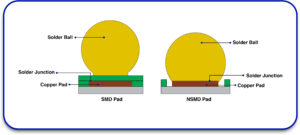
2. Surface-Mount Pads
- Applied to new high-density PCBs.
- Components are mounted directly to flat pads without going through holes.
- Take up less space, hence suitable for flexible PCB manufacturing.
Role of PCB Pads in Circuit Design
An adequate PCB pad guarantees:
- Solid component attachments to withstand everyday use.
- Effective soldering with the right amount of solder or no solder at all.
- Clear electrical conductivity to pass signals.
- Good heat dissipation to avoid component failure.
- Cold solder joints, poor mechanical connections, and signal integrity problems can be caused by poor pad design.
PCB Pad Structure: Important Elements
All Pad PCB designs should have these structural elements:
1. Pad Shape and Size
- Pads are available in round, rectangular, oval, and custom shapes.
- Size varies with component lead size and soldering technique.
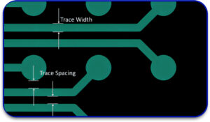
2. Pad Spacing
- Poor spacing can lead to short circuits or poor connections.
- Maintain adequate clearance between pads for better reliability.
3. Pad Plating
- Common plating materials include gold, silver, and tin.
- ENIG (Electroless Nickel Immersion Gold) is widely used for better conductivity and durability.
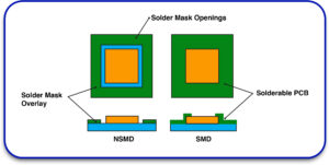
4. Solder Mask
- A protective layer that prevents solder bridging between adjacent pads.
- Essential for high-density PCB layouts.
Development Process of PCB Pads
The PCB pad development process follows a series of crucial steps to ensure reliable connections and durability.
Step 1: Identifying Component Requirements
Prior to pad design, engineers study component specifications like:
- Pin pitch (pin-to-pin distance).
- Lead type (through-hole or surface mount).
- Current and thermal needs.
Step 2: Choosing the Pad Size and Shape
Pad sizes should:
- Mimic the component footprint.
- Leave sufficient room for soldering without short circuits.
- Optimize for automated PCB assembly.
Step 3: Determining Pad Placement and Spacing
Correct pad spacing avoids:
- Solder bridges that lead to shorts.
- Overheating due to inadequate heat dissipation.
- Mechanical stress could reduce solder joint strength.
Step 4: Applying Solder Mask and Plating
Solder mask prevents oxidation and ensures accurate solder application.
- Plating guards pads and improves conductivity.
Step 5: Running Design Rule Checks (DRC)
Engineers execute DRC checks before the layout is finalized to ensure:
- Proper pad dimensions.
- Suitable clearance between pads.
- Correct alignment with component leads.
Best Practices for Pad PCB Design
1. Adhere to Industry Standards
- Utilize IPC-7351 guidelines for standardized pad design.
- Comply with the requirements of custom PCB manufacturing.
2. Sizing Pads for Soldering
- Too small pads produce weak joints.
- Too large pads create excessive solder buildup.
3. Provide Proper Thermal Relief
- In power applications, thermal relief pads assist with heat dissipation.
- Prevent overheating that may destroy components.
4. Keep Good Pad-to-Trace Connection
- The pad-to-trace connection should be wide enough for good conductivity.
- Avoid using thin traces that may lead to signal integrity problems.
5. Utilize Staggered Pads for High-Density PCBs
- Staggered pads during flexible PCB production prevent solder bridges.
- Enhances mechanical strength in multilayer boards.
Mistakes to Avoid in PCB Pad Design
1. Misaligned Pads
- Poor alignment of pads results in poor soldering and weak connections.
- Always check pad positioning using PCB design software simulations.
2. Insufficient Pad Clearance
- Pads that are too close together will result in shorts.
- Adhere to minimum clearance specifications based on manufacturing tolerances.
3. Poor Heat Dissipation
- Pads with inadequate thermal relief can overheat.
- Employ thermal vias, and copper pours to control heat.
4. Improper Pad Plating
- Selecting the wrong plating material can shorten pad life.
- Gold and ENIG plating are optimal for high-reliability PCBs.
How Blind Buried Circuits Can Assist
At Blind Buried Circuits, we offer custom PCB production and flexible PCB production, providing high-quality Pad PCB design for different applications.
- Professional PCB pad design to maximize performance and longevity.
- High-precision production of intricate and high-density PCBs.
- Compliance with industry standards for perfect production.
Seeking trusted PCB production with the optimal pad structure design? Get in touch with us today and begin your next PCB project!
Pad PCB design is an essential component of PCB layout and has a direct influence on soldering quality, longevity, and circuit functionality. By observing best practices, employing appropriate PCB pad structures, and maintaining the proper spacing and plating, you can eliminate typical PCB design errors and build extremely reliable circuit boards.When working on custom PCB manufacturing or flexible PCB fabrication, make sure to collaborate with an experienced PCB board manufacturer like Blind Buried Circuits to ensure your design meets industry standards. Have questions about PCB pad development? Let’s discuss your project today!


