An ideal PCB design is crucial for a circuit board’s reliability, functionality, and manufacturability. An efficient PCB board layout can save time and money and enhance performance. Whether you are developing a prototype or a complex multi-layered board, a structured PCB design checklist will help your circuit be optimized for functionality, signal integrity, and manufacturability.
This guide has provided a comprehensive checklist on PCB design considering component placement to final verification and optimization. It will help streamline the process and enhance cooperation with a PCB assembly company to achieve the expected seamless PCB board assembly manufacturing.
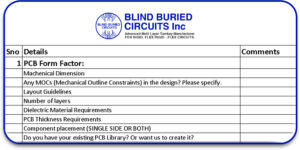
Checklist for PCB Design
A PCB design checklist helps to avoid mistakes that cause signal issues, manufacturing delays, or real-world omissions. In addition, using a checklist assists in Averting design gaps pre-manufacturing, Optimizing the placement of electrical components, Avoiding conflicts with PCB assembly services, Enhancing reliability and ease of manufacturability, and Accelerating prototyping and mass production. By following a checklist, designers may be able to generate PCBs in the easiest way while considering quality alongside cost.
Complete Checklist for Design of PCB
1.State the requirements for PCB first
Start with the simpler step: write down all the specifications that you want your PCB design to meet to serve the goal of the project. For reference, complete the following items:
- State the intended usage (consumer electronics, medical, automotive, aerospace, etc.).
- Decide how many layers you need (single-layer, double-layer, multi-layer PCB).
- Describe the size and shape of the board so it fits within the product casing.
- Identify power and signal levels required for stable performance.
- Establish environmental conditions such as temperature, humidity, and mechanical impacts.
Covering all these aspects will ensure informed design decisions and an effortless experience with the PCB assembly company.
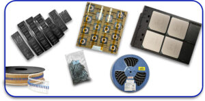
2. Choosing Boards and Components
The step involves the selection and placement of components based on their performance, reliability, and assembly integration.
- Avoid supply component issues by using readily available stock components.
- Ensure footprints are correctly matched to the PCB layout.
- Place high-frequency components next to their circuits to reduce signal delay.
- Separate analog and digital components to minimize interference.
- Avoid placing components at the extreme edge to prevent mechanical damage.
- Position heat-producing components near heat sinks or airflow areas.
Correct component placement enhances the device’s electrical performance and eases manufacturability, enabling PCB board assembly teams to effortlessly produce quality boards.
3. Power and Ground Plane Design
- The divide area ensures the scalability of the voltage in the circuit and nullifies noise within the plane.
- Improve signal integrity by using dedicated ground and power planes.
- Minimize resistance by designing short and wide power traces.
- Position decoupling capacitors at the power pins of the IC to filter out noise from the system.
- Avoid ground loops by implementing star grounding techniques.
An effective power and ground plane layout increases signal stability, reduces EMI (Electromagnetic Interference), and enhances the board’s functionality.
Learn About: Best EMI and RF Sheilding Methods for Flex PCBs
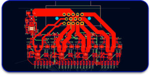
4. Signal Routing Best Practices
For signal routing to be effective:
- Minimize surrounding interference, maintain constant impedance, and ensure high-speed performance.
- Use direct routing for better signal fidelity instead of long, convoluted trace paths.
- Employ differential pairs for USB, HDMI, and RF circuit signals.
- Maintain a consistent trace width to simplify impedance control.
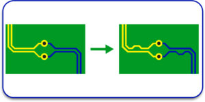
- Avoid 90-degree sharp corners; use 45-degree angles instead.
- Ensure sufficient gap between traces to prevent short circuits.
Good signal routing minimizes crosstalk, noise, and unwanted coupling, resulting in a stable PCB circuit diagram.
5. Via And Layer Stack Up Design
Vias are essential for signal flow and thermal management, as they connect different layers of the PCB.
- For regular connections, use through-hole vias.
- For complex HDI PCBs, use blind and buried vias.
- In high-density designs, microvias may be used to save space.
- Adapt trace width and spacing to manufacturing limitations.
Adequate heat dissipation, signal integrity, and manufacturing efficiency are achieved with a well-planned layer stackup.
Learn About: Microvia Design Essentials: Enhancing PCB Durability and Functionality
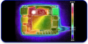
6. Thermal Management Consideration
Extended life and reduced overheating of PCBs are achieved with efficient thermal management.
- Use thermal vias to conduct heat away from power components.
- Place heat sinks or copper pours under high-power devices.
- Provide adequate spacing for heat-sensitive components.
- Implement thermal relief patterns on vias to prevent heat buildup.
Lack of heat dissipation can lead to PCB component overheating, causing failures or a shortened lifespan.
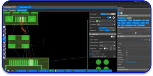
7. Design Rule Check (DRC) and Electrical Rule Check (ERC)
Automated DRC and ERC checks should be conducted before sending your design for manufacturing. These checks are essential in preventing costly design errors and delays in production.
- DRC (Design Rule Check): Ensures the PCB complies with manufacturing limits, such as trace widths, clearances, and hole dimensions.
- ERC (Electrical Rule Check): Detects issues like short circuits, floating nets, and signal contention.
- Check netlist connections to confirm that the schematic matches the PCB layout.
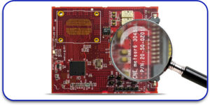
8. Silkscreen and Documentation
- Silkscreen markings should be added for quick identification of component positions.
- Correct labeling and documentation assist assembly teams in accurately building and testing their PCBs.
- Include essential details such as polarity marks, reference designators, test points, Gerber files, BOM (Bill of Materials), and assembly drawings.
- These documents enable assembly manufacturers to construct the PCB accurately, without ambiguity or errors.
9. Final Design Verification and Prototyping
- Finalize verification and testing before transitioning to mass production.
- Engage your PCB supplier to review the design for manufacturability.
- Perform simulations to confirm expected performance.
- Build a prototype to test it in real life.
Prototyping reduces the cost of rework by allowing issues to be identified and amended before production begins.
A checklist detailed in this guide ensures that the PCB design process is streamlined, cost-effective, and high-quality. Adhering to the checklist guarantees that the design is trustworthy and easy to manufacture and assemble. Here at Blind Buried Circuits, we focus on custom PCB fabrication and assembly, assuring that your designs are expertly fabricated to industry standards. Our experts are ready to assist you whether you want custom PCBs, prototypes, or bulk production.
To receive professional assistance and learn how to implement your PCB designs effectively, reach out to us now.


