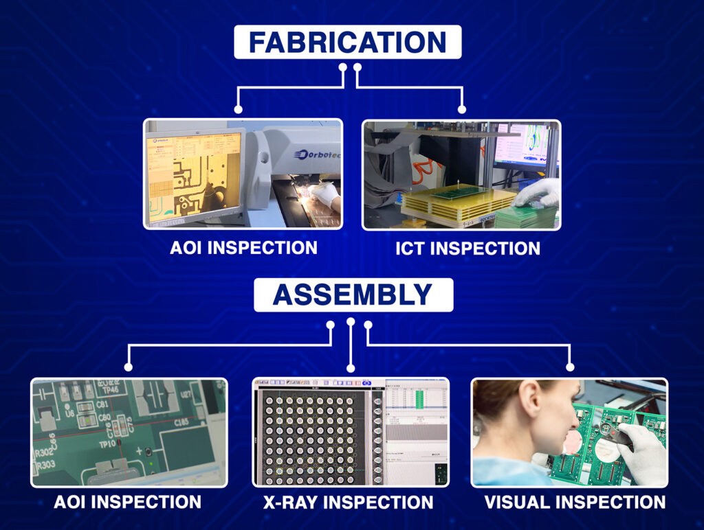
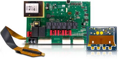
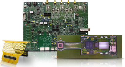
For PCB designers and electronic engineers, creating a reliable, efficient, and functional circuit board begins with accuracy. A minor mistake in the PCB layout can result in functionality issues, increased costs, or costly redesigns. That’s where PCB layout design tools come into play. These specialized tools help automate and simplify complex design tasks, enabling you to achieve a higher level of precision and accuracy throughout the design process.
The Role of PCB Layout Design Tools in Improving Accuracy
PCB layout design tools are sophisticated software programs that assist in the creation and validation of PCBs. These tools cover various aspects of the PCB design process, including schematic capture, component placement, routing, and design validation. By utilizing advanced algorithms, automation features, and real-time feedback, these tools help engineers and designers eliminate human errors and optimize their designs for both performance and manufacturability. When working with a reliable PCB manufacturer, these tools ensure that the final design is precisely translated into high-quality, functional circuit boards.
Key processes where PCB layout design tools improve accuracy include:
- Design Rule Checks (DRC): Automatically check if the design meets electrical and manufacturing standards.
- Trace Routing: Ensuring that traces are properly routed to prevent signal integrity problems.
- Signal Integrity Analysis: Checking the electrical performance of the design, including minimizing noise and interference.
- Component Placement: Ensuring components are optimally placed to minimize conflicts and optimize space.
Let’s dive deeper into these features and understand how they improve accuracy.
Key Features of PCB Layout Design Tools to Improve Accuracy
Design Rule Check (DRC)
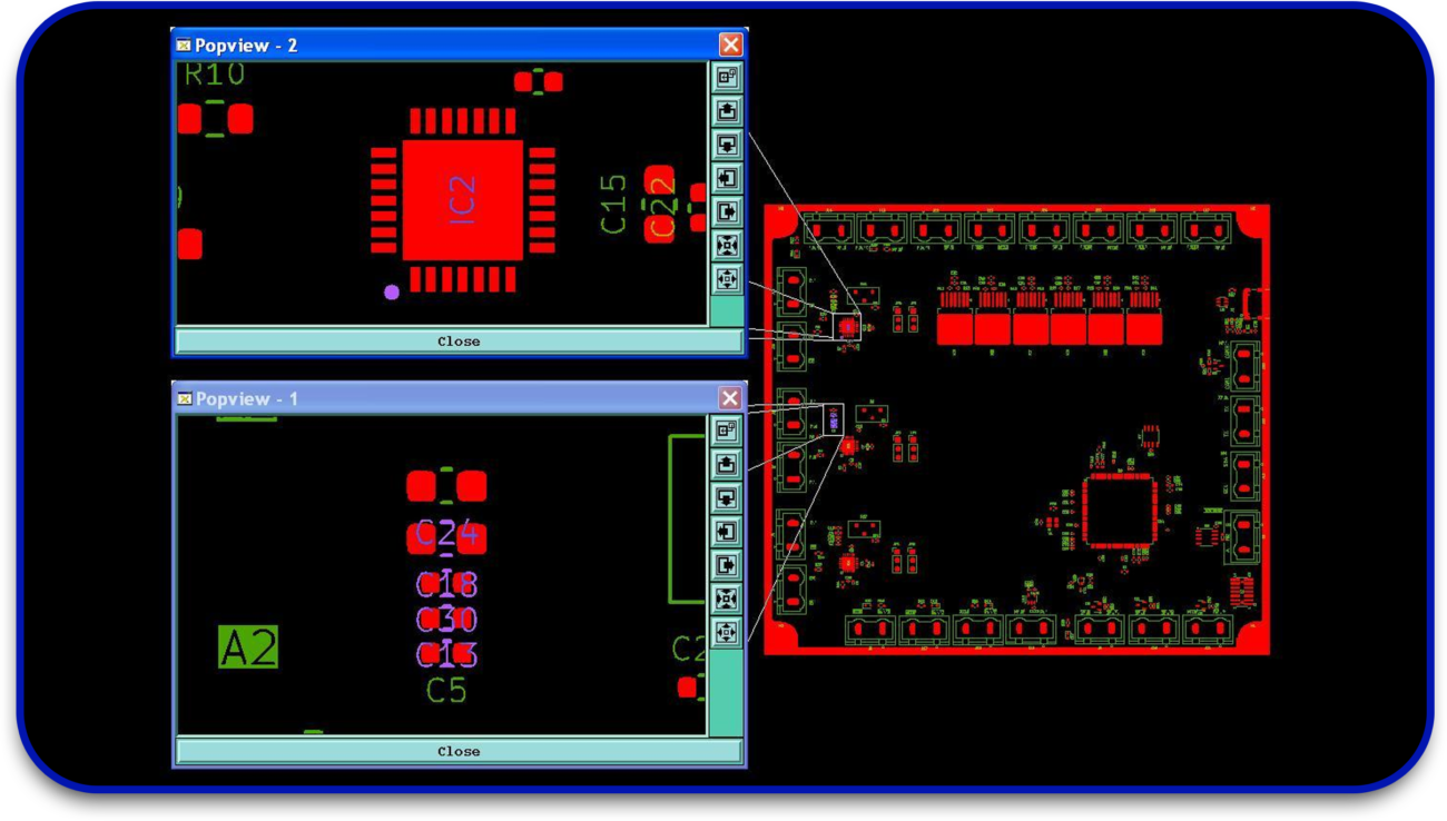
One of the most fundamental aspects of PCB layout design tools is the Design Rule Check (DRC). DRC automatically checks the layout against a predefined set of design rules, such as trace width, component spacing, via sizes, and layer constraints. Violations are flagged immediately, allowing designers to correct them before they cause issues in the final product. For example, if a trace is too thin and cannot carry the required current, the DRC will highlight this as an error, preventing potential failure in the circuit.
Running DRCs throughout the design process, especially during the initial stages and before finalizing the design, is crucial. It ensures the layout is electrically sound, manufacturable, and meets industry standards, avoiding common mistakes like shorts, unconnected pins, or signal degradation.
Signal Integrity Analysis
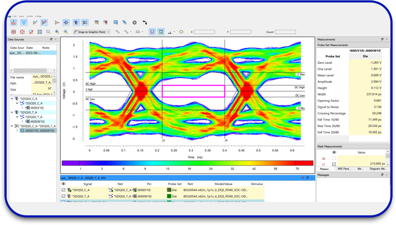
Signal integrity is critical to ensuring the proper functioning of high-speed circuits. Improper trace routing, insufficient grounding, or poor component placement can lead to problems such as crosstalk, noise, and signal reflections that degrade the PCB’s performance.
Modern PCB design tools like Altium Designer or Cadence Allegro come equipped with Signal Integrity Analysis features that help simulate and test signal behavior across the board.
By using these analysis tools, you can identify problems like excessive noise, improper impedance matching, or delays in signal transmission. This allows designers to make changes before physical prototypes are produced, thus improving the accuracy of the final PCB and its electrical performance.
3D Visualization
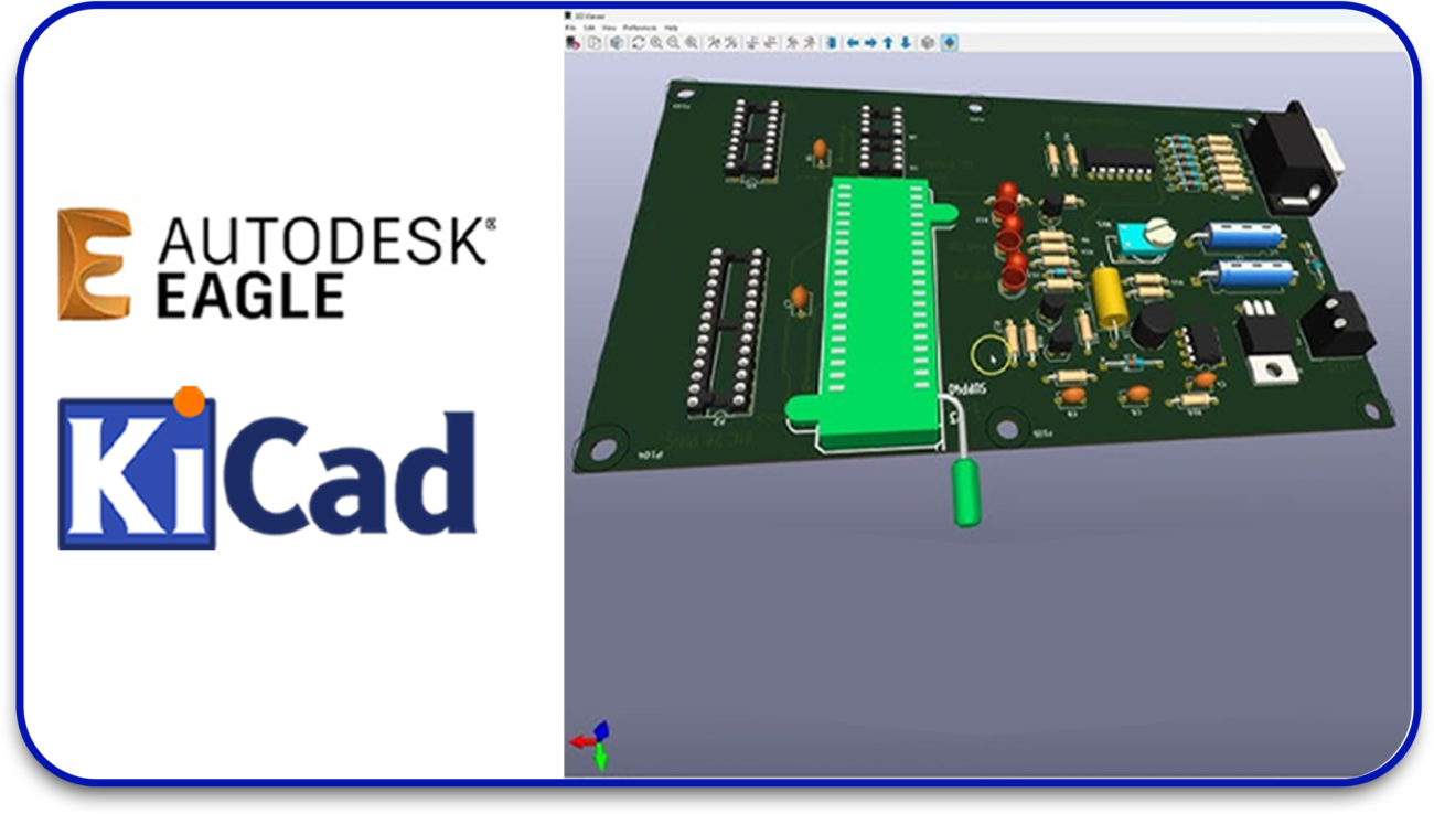
One of the most useful advancements in PCB design tools is 3D visualization. Tools like Autodesk EAGLE and KiCad provide 3D modeling capabilities, allowing you to view the layout in three dimensions.
This visualization enables designers to detect potential issues that would otherwise go unnoticed, such as mechanical interference, component clashes, or overcrowded areas. It also ensures the board layout adheres to the required height and clearance constraints.
By seeing the design in 3D, engineers can optimize component placement, minimize the risk of future assembly problems, ensure that the board fits within the enclosure, and allow for better thermal management.
Auto-Routing and Interactive Routing
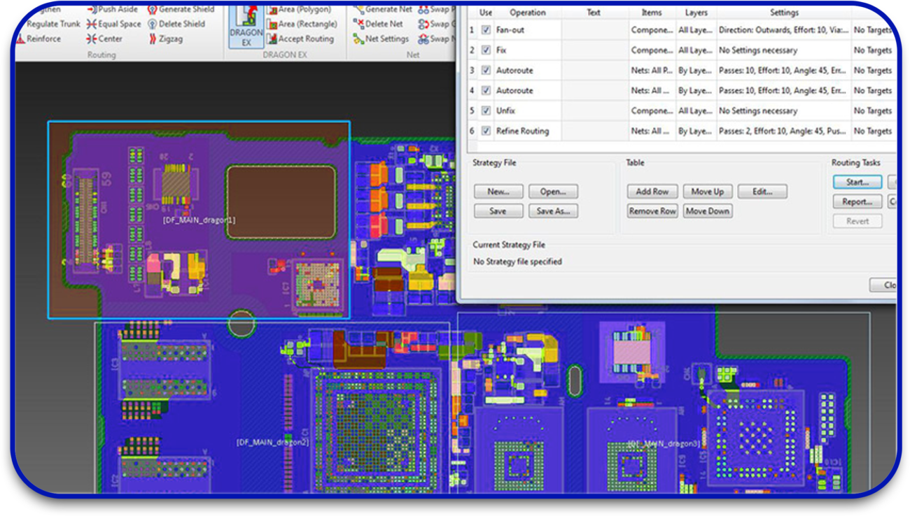
PCB layout design tools can also help automate trace routing. Auto-routing features use algorithms to automatically determine the best path for traces, taking into account various factors like component placement, trace width, and current-carrying capacity. This automation reduces the possibility of routing errors and ensures that the traces are optimized for both performance and manufacturability.
However, while auto-routing can save time, designers still need to manually review and adjust the routed traces. Interactive routing features let engineers make manual adjustments to auto-generated routes, ensuring the design meets specific needs like minimizing crosstalk or optimizing routing paths. This combination of auto-routing and interactive routing improves accuracy by eliminating human errors in complex routing and optimizing the design for real-world performance.
Simulation and Testing
Simulation tools integrated into PCB design software allow you to test your circuit design’s performance without physically building a prototype. Simulations can check for power integrity issues, temperature-related problems, and electrical failures.
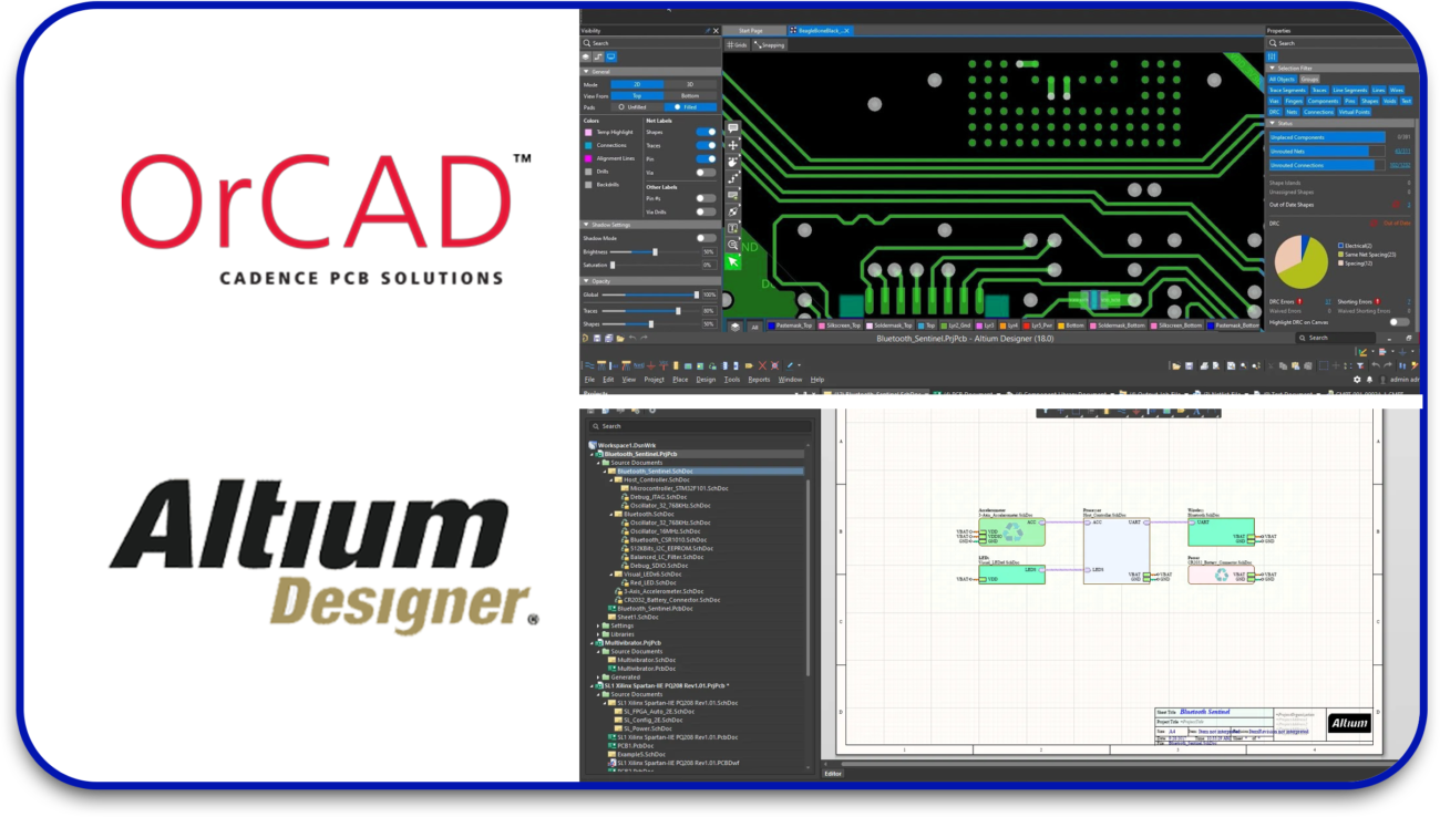
Many modern tools, such as OrCAD PCB Designer or Altium Designer, offer simulations that include thermal analysis, power distribution analysis, and EMI (electromagnetic interference) checks.
Testing the design before fabrication helps identify potential problems that could impact accuracy or functionality. For instance, if the simulation shows that a trace overheats or a component is placed incorrectly, it’s much easier to address these issues in the virtual design phase than after physical fabrication.
Cadence Allegro PCB Designer:
- Allegro provides advanced routing capabilities, signal integrity analysis, and powerful DRC tools. It’s designed for high-speed, high-frequency designs, making it ideal for engineers working on complex PCBs.
Autodesk EAGLE:
- EAGLE is a popular choice for hobbyists and small businesses due to its affordability and user-friendly interface. It includes essential features like auto-routing, component libraries, and DRC, making it an excellent tool for precise PCB design.
KiCad:
- KiCad is an open-source PCB design tool that’s completely free to use. Despite being free, it offers professional-grade features like 3D visualization, schematic capture, and DRC, making it a great option for engineers working on both simple and advanced projects.
OrCAD PCB Designer:
- OrCAD is a robust PCB design suite offering tools for schematic capture, PCB layout, signal integrity analysis, and simulations. Its user-friendly interface and integration with other Cadence tools make it a top choice for professionals.
Why Accuracy is Crucial in PCB Design?
Inaccurate PCB designs can lead to a range of issues, including:
- Increased Manufacturing Costs: Errors such as misrouted traces, incorrect component placement, or design rule violations can lead to costly revisions and delays.
- Electrical Failures: Inaccurate trace routing, signal integrity problems, and improper component selection can result in poor electrical performance or circuit malfunction.
- Reliability Issues: PCBs with accuracy issues may not function as expected over time, leading to reliability concerns, especially in mission-critical applications like medical devices, aerospace, or automotive electronics.
By ensuring your PCB design is as accurate as possible from the beginning, you minimize the risk of these problems, improving both the design’s efficiency and the final product’s reliability.
Common PCB Design Tools and Their Features
| Tool | Features | Best For |
| Altium Designer | Advanced design rule checks, 3D visualization, signal integrity analysis | Complex designs and professionals |
| Eagle PCB | Automated error checking, large component library | Small to medium designs, hobbyists |
| KiCad | Open-source, 3D visualization, multi-layer support | Beginners, educational projects |
| OrCAD | Analog and digital design capabilities, advanced error checking | Professional and industrial applications |
PCB layout design tools play a vital role in improving circuit design accuracy. They help eliminate human errors, ensure compliance with design rules, simulate real-world performance, and optimize the layout for manufacturability. By using these tools, PCB designers and electronic engineers can streamline the design process, reduce costs, and create more reliable, high-performance circuit boards.
As PCB design continues to grow more complex, using advanced tools like Altium Designer, Cadence Allegro, or KiCad becomes essential for maintaining precision and accuracy. These tools not only enhance productivity but also ensure that the final product meets electrical, mechanical, and manufacturing requirements with minimal risk of failure.
Investing in the right PCB layout design tools is crucial for any engineer who wants to produce high-quality, accurate circuit designs that meet performance and manufacturing standards.
For more information on our PCB manufacturing and assembly services, visit Blind Buried Circuits

