Objective
This blog explains how PCB component placement affects design quality, assembly success, thermal control, and signal performance. The goal is to help designers make better placement decisions before routing begins. Good placement saves time, reduces mistakes, and makes the full board easier to build and test.
Key Takeaways
- Good PCB component placement makes routing easier and cleaner.
- Poor placement can create signal noise, heat problems, and assembly defects.
- Strong component placement guidelines that PCB teams follow can reduce rework.
- Smart spacing and part orientation improve assembly speed and inspection.
- Good decoupling capacitor placement supports power stability.
- Simple SMT component placement rules can prevent costly production issues.
Table Of Contents
- Introduction: Why Component Placement Is More Important Than Most Designers Think
- Understanding The Basics Of PCB Component Placement
- Essential PCB Component Placement Rules Every Designer Should Know
- PCB Component Placement Guidelines For Thermal Management
- Component Placement Guidelines For Signal Integrity
- PCB Component Placement For Assembly Efficiency
- PCB Component Placement Guidelines For Manufacturability
- High-Density And Complex Board Placement Strategies
- Common PCB Component Placement Mistakes And How To Avoid Them
- PCB Component Placement Checklist Before You Route
- Tools And Features That Help With Component Placement
- Conclusion
- FAQs
1. Introduction: Why Component Placement Is More Important Than Most Designers Think
A lot of PCB problems start before routing.
They start when parts are placed without a clear plan.
A designer may focus on getting every component onto the board first. That seems normal. But if the placement is rushed, the routing becomes harder, the board gets noisier, and the assembly process becomes less reliable. Good routing cannot fully fix poor placement.
That is why PCB component placement matters so much.
Placement affects almost everything that follows. It affects signal flow, power delivery, heat movement, board size, manufacturing yield, test access, and even repair work later. When placement is done well, the rest of the design process feels more controlled. When placement is done poorly, the whole board starts fighting back.
At Blind Buried Circuits, this matters even more on dense and advanced boards. Tight designs leave less room for placement mistakes.
What Goes Wrong When Placement Is Done Poorly
Poor placement often causes problems that are not obvious at first.
These problems can include:
- long and messy traces
- weak return paths
- noisy analog sections
- poor decoupling
- assembly crowding
- blocked test points
- hard-to-reach connectors
- heat trapped near sensitive parts
- difficult rework
A board can still look complete on screen and still be weak in real life. That is the danger.
How Good Placement Affects Both Design And Assembly
Good placement helps the designer and the assembly team at the same time.
It can:
- shorten routing paths
- reduce layer changes
- support cleaner signal flow
- improve airflow
- make pick-and-place easier
- improve inspection access
- reduce soldering defects
- Save time during debug
That is why the strong component placement guidelines PCB teams use are not just layout preferences. They are practical design rules.
2. Understanding The Basics Of PCB Component Placement
What Is Component Placement In PCB Design?
PCB component placement is the step where the designer decides where each part will sit on the board before routing begins.
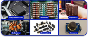
This includes:
- integrated circuits
- resistors
- capacitors
- inductors
- connectors
- sensors
- power devices
- switches
- test points
Placement is not random. It must support how the circuit works, how the board will be assembled, and how the final product will fit inside its enclosure.
The Relationship Between Placement, Routing, And Signal Integrity
Placement and routing are closely connected.
If the right parts are close to each other, routing becomes shorter and simpler. If they are placed too far apart, the traces become longer. Longer traces can create more resistance, more inductance, and more chances for noise or signal quality problems.
This is especially important in high-speed designs.
Some of the best high-speed PCB placement tips are really placement habits, not routing tricks. Keep fast paths short. Keep clocks controlled. Keep decoupling close. Keep return paths clean.
Good routing usually begins with good placement.
Placement Vs. Component Management — How They Work Together
Placement and component management are not the same thing, but they support each other.
Component management helps keep:
- correct footprints
- correct symbols
- accurate 3D models
- correct package heights
- sourcing data
- part status
Placement uses that data to make smart decisions.
If a footprint is wrong, placement can be wrong. If a part height is wrong, the board may not fit the enclosure. If a connector model is wrong, the mechanical position may fail.
This is why part data and placement must work together.
3. Essential PCB Component Placement Rules Every Designer Should Know
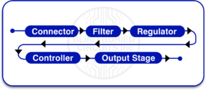
Follow The Signal Flow Direction
A simple rule helps a lot: place parts in the order the signal moves.
For example, the flow might be:
connector → filter → regulator → controller → output stage
This makes the design easier to understand and easier to route.
Keep Related Components Close Together
Components that support the same function should stay close.
Examples include:
- microcontroller and crystal
- regulator and its input/output capacitors
- driver and transistor
- amplifier and feedback network
This reduces trace length and helps the circuit behave more like it should.
Separate Analog And Digital Components
Analog circuits are usually more sensitive to noise. Digital circuits can switch quickly and create noise.
If these two sections are mixed carelessly, the analog side can suffer.
Keep them separated with a clear layout plan. This is one of the most useful placement rules for mixed-signal boards.
Maintain Proper Clearance Between Components
Spacing matters.
If components are too close, the board may become hard to assemble, inspect, or rework. Tight spacing can also affect heat flow and solder joint quality.
Proper clearance depends on package size, assembly process, voltage needs, and tool access. There is no single spacing rule for every board, but cramped layouts usually cause trouble.
Orient Components Consistently For Easier Assembly
Consistent orientation makes life easier.
If polarized parts face the same direction and reference markings are readable in a consistent way, the board becomes easier to assemble, inspect, and troubleshoot.
This is one of the simplest SMT component placement rules, and it makes a real difference.
4. PCB Component Placement Guidelines For Thermal Management
Identify And Isolate Heat-Generating Components
Some components naturally run hot.
These often include:
- voltage regulators
- MOSFETs
- power resistors
- processors
- LEDs
- power modules
These parts should be identified early and placed with thermal planning in mind.
Do not scatter them randomly.
Use Thermal Vias and Copper Pours Strategically
Placement alone does not solve heat problems, but it sets up the thermal strategy.
Thermal vias can move heat into the inner or bottom layers. Copper pours can help spread heat. But both only work well when the hot parts are placed in sensible locations.
A hot component boxed into a crowded corner is harder to cool.
Placing Heat-Sensitive Parts Away From Hot Zones
Some parts do not like heat.
These may include:
- sensors
- crystals
- precision references
- analog ICs
- batteries
- certain connectors
Do not place them too close to power parts or heat sinks.
Airflow Direction And Its Impact On Component Placement
If the board works inside a system with fans or natural airflow, placement should respect that direction.
Hot components should not block cooling for other parts. Tall parts should not create unwanted thermal shadows over sensitive devices.
Thermal planning starts with placement, not with wishful thinking later.
5. Component Placement Guidelines For Signal Integrity
Minimizing Trace Length For High-Speed Signals
One of the most important high-speed PCB placement tips is to keep fast signal paths short.
This matters for:
- clock lines
- memory buses
- USB
- PCIe
- RF signals
- fast serial links
The longer the path, the greater the chance of reflections, delay issues, and unwanted coupling.
Placing Decoupling Capacitors Close To Power Pins
This rule is simple and important.
Place decoupling capacitors as close as possible to the power pins they support.
Do not leave them floating far away with long traces. That weakens their job. Their purpose is to provide quick local current and help reduce power noise.
Managing Return Current Paths
Every signal needs a return path.
If the return path is broken or forced to take a long route, signal quality gets worse. Placement affects this because it shapes where traces and reference planes will go.
Good placement supports direct and predictable current return.
Avoiding Crosstalk Between Signal Lines
Noisy lines should not be packed too closely beside sensitive lines.
Keep a distance between:
- clock lines and analog inputs
- switching nodes and sensor traces
- RF paths and digital buses
This reduces unwanted coupling and improves stability.
6. PCB Component Placement For Assembly Efficiency
Placing Components On One Side Vs. Both Sides Of The Board
Single-sided placement is usually easier to assemble and inspect. It may also reduce cost.
But not every board has that luxury. Double-sided placement can save space, especially on small or dense designs.
The choice depends on board size, complexity, cost target, and assembly process.
Grouping SMD And Through-Hole Components Correctly
Surface-mount and through-hole parts often require different handling during assembly.
It helps to place them in a planned way instead of mixing them without thought. This supports a smoother manufacturing flow.
Meeting Pick-And-Place Machine Requirements
Machines need space and visibility.
Good placement supports:
- nozzle access
- stable part pickup
- clear fiducials
- repeatable orientation
- safe spacing
A board that is hard for the machine is usually hard for production.
Leaving Space For Soldering Iron And Rework Access
Not every board will pass through production without issues. Sometimes a part needs to be reworked or replaced.
If the layout leaves no room for tools, rework becomes slow and risky. A good design should leave enough practical access around important components.
Avoiding Tombstoning Issues With Passive Component Placement
Small passives can tombstone when solder forces become unbalanced.
Placement alone is not the only cause, but it plays a part. Uneven thermal conditions, poor pad design, and awkward local copper can make the risk worse.
This is why SMT component placement rules matter even for tiny passive parts.
7. PCB Component Placement Guidelines For Manufacturability (DFM)
What Is Design For Manufacturability, and Why It Starts At Placement
Design for manufacturability means designing the board so it can be built reliably and repeatedly.
DFM does not begin at the factory. It begins during placement.
Component Spacing Rules For Wave And Reflow Soldering
Different soldering methods need different spacing behavior.
Components need enough room for:
- solder paste printing
- proper heating
- solder joint formation
- inspection
- cleaning, when needed
Crowded placement can hurt yield.
Fiducial Marker Placement For Assembly Alignment
Fiducials help assembly equipment align the board correctly.
Their placement should be planned early so they remain clear and useful.
Board Edge Clearance Rules
Parts placed too close to the edge may suffer during depaneling, handling, or enclosure fitting.
Keep a sensible clearance from:
- board edges
- mounting holes
- break tabs
- rails
Panel And Breakaway Tab Considerations
If the board will be panelized, component placement must respect tab locations and tool paths.
Fragile parts near break points are a bad idea.
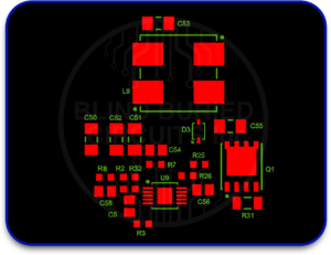
8. High-Density And Complex Board Placement Strategies
Handling BGA And Fine-Pitch Components
BGA and fine-pitch parts demand careful thought.
They need:
- escape routing space
- via planning
- thermal planning
- inspection awareness
Do not place them casually in areas that cannot support fanout.
Placement Tips For Multi-Layer Boards
Multi-layer boards give more routing freedom, but they also demand better placement discipline.
Think about how the part connects to reference planes, power layers, and nearby interfaces.
Managing Connector And Port Placement On Board Edges
Connectors usually belong near the board edge.
If they are placed too far inboard, the product may become harder to assemble into its case or harder to use in the real world.
Stacking And Shielding Sensitive Components
Some sections need isolation or shielding.
This is common in:
- RF layouts
- sensitive analog circuits
- mixed-signal designs
- noisy power systems
Placement should support that separation.
9. Common PCB Component Placement Mistakes And How To Avoid Them
Designers often run into the same avoidable mistakes.
These include:
- placing connectors away from the board edge
- ignoring part height limits
- placing decoupling capacitors too far from IC pins
- blocking test points
- Crowding hot components near sensitive parts
- forgetting enclosure limits until late
- creating awkward rework access
The fix is simple in theory. Think earlier. Review placement harder. Do not treat placement as a quick first draft.
10. PCB Component Placement Checklist Before You Route
Before routing begins, verify these points:
- signal flow is logical
- Power sections are grouped correctly
- Decoupling capacitors are close to the IC pins
- Analog and digital areas are separated
- High-speed paths are short
- connectors are placed correctly
- thermal zones are planned
- Board edge clearance is checked
- fiducials are clear
- test points are accessible
- tall components fit mechanical limits
- Rework access is possible
11. Tools And Features That Help With Component Placement
Design Rule Check (DRC) For Placement Errors
DRC tools help catch:
- spacing violations
- overlaps
- edge clearance issues
- room violations
They do not replace good judgment, but they help.
3D Viewer For Mechanical Fit Verification
A 3D view helps the designer check:
- connector fit
- height clearance
- enclosure limits
- collision risk
This is especially helpful on compact products.
Interactive Placement Tools In Modern PCB Software
Modern PCB tools can help with:
- component alignment
- room-based layout
- class grouping
- push-and-move behavior
- spacing feedback
These features save time when used well.
How Component Management Services Support Better Placement Decisions
Better placement depends on accurate data.
If the footprint, 3D model, or part height is wrong, placement decisions become risky. Good component management supports good placement because the designer can trust the part data.
12. Conclusion
Good PCB component placement is one of the clearest signs of a disciplined board design.
It affects signal quality, thermal behavior, assembly ease, test access, manufacturability, and long-term reliability. A board that starts with smart placement is easier to route and easier to build. A board that starts with weak placement usually creates problems all the way through the process.
That is why Blind Buried Circuits treats placement as a core part of board quality, not just an early draft step.
CTA Quote: Better boards begin with better placement. Clean part placement makes routing easier, assembly smoother, and final performance more reliable.
FAQs
Q1. What Is The First Step In PCB Component Placement?
Start with the fixed parts first. These usually include connectors, mounting holes, large ICs, power sections, and any parts tied to the enclosure.
Q2. How Much Clearance Should Be Left Between Components On A PCB?
There is no single answer for every board. Clearance depends on package size, voltage, manufacturing method, and rework needs. The key is to leave enough space for reliable assembly, inspection, and service.
Q3. Why Should Analog And Digital Components Be Separated On A PCB?
Digital circuits can create switching noise. Analog circuits are more sensitive. Separation helps reduce unwanted noise coupling.
Q4. What Is The Best Placement Strategy For Decoupling Capacitors?
Place them as close as possible to the IC power pins they support. Keep the current loop short and direct.
Q5. How Does Component Placement Affect PCB Assembly Cost?
Better placement can reduce assembly trouble, inspection difficulty, rework time, and defect risk. That can help lower the total build cost.
Q6. Should All Components Be Placed On One Side Of The Board?
Not always. One side is simpler for assembly, but many boards need both sides because of size or density limits. The right choice depends on the design goals.


