Have you thought about how some electronics devices are capable of achieving a high-density connection in such a compact space? Or how does a tiny chip get firmly and reliably mounted on a circuit board without any visible pins? The answer often comes from a specific technology known as Ball Grid Array or BGA.
Suppose you are familiar with the term BGA but do not know what it stands for or why it ‘s essential. In that case, this blog will explain to you the concept from the beginning, which includes the definition, the assembly process, and BGA X-Ray inspection in BGA assembly.
What Is A BGA in PCB Assembly?
A BGA or a Ball Grid Array is a type of packaging for an electronic chip which consists of small balls of solder arranged in a grid form on the chip’s bottom surface. These balls provide solder joints for the chip to solder to the PCB. In comparison to other types of chip packaging, which have pins or legs soldered on, BGA-mounted chips offer denser soldering areas in a compact size. This increases the size and speed of the circuit, resulting in BGA’s wide usage in modern electronics.
The process of assembling PCBs and adding BGA chips on top of them is called BGA PCB assembly. BGA PCB assembly requires great precision and control since every single solder ball needs to be perfectly connected without any flaws.

Why is BGA Used in PCB Manufacturing?
BGA technology aids in the PCB manufacturing assembly for various key reasons:
- High-density connection: Compared to the traditional pin soldering method, BGA technology permits an increased number of electrical connection points, resulting in greater solder ball connections.
- Enhanced functionality: Signal speeds and interference are optimized due to the shorter electrical pathways.
- Reduced PCB dimension: BGA technology contributes to space saving, which results in more compact devices.
- Greater durability: Under stress, BGA solder joints are more resilient and are less likely to break.
Due to these advantages, BGA packages are widely adopted in smartphones, laptops, and gaming consoles.

The BGA PCB Assembly Process: Step by Step
BGA assembly on a PCB requires careful execution of several steps to ensure flawless functionality:

PCB Pad Solder Masking:
The BGA solder pads are positioned on the PCB, and a thin layer of solder paste is applied to the solder pads. Solder paste is a combination of tiny solder particles and flux, which aids in solder adhesion and fluidity.
BGA Placement:
The BGA chip is positioned on the PCB using an automated pick and place machine that makes sure the solder balls will match the required solder paste on the pads.
Reflow Soldering:
The BGA soldered PCB is placed in the reflow oven, where the board is heated to a specific temperature to bring the solder balls and solder paste to a molten state to facilitate strong electrical and mechanical connections.
Cooling:
The PCB goes through a rapid cooling stage to solidify the solder joints after overheating.
Inspection:
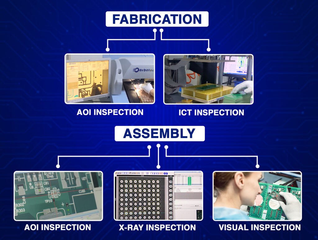
BGA X-Ray inspection systems are utilized to inspect BGA chip parts to provide inspection and quality verification on the BGA solder joints out of sight.
Testing and Cleaning:
Leftover flux and contaminants are purged while other systems conduct check-ups to verify the system components are fully operational.
To enhance durability, the assembled BGA connections undergo thorough procedures.
What Is BGA X-Ray Inspection and Why Is It Important?
The primary issue with BGA assembly is the fact that solder joints are concealed with the chip, meaning that visually assessing the connections to the solder balls and the risk of cold joints, bridging, or voids is impossible.
This is where you can use BGA x-ray inspection. This method uses X-rays to look inside the chip to see the solder joints that are not visible. This is useful in identifying:
- Missing or insufficient solder balls
- Solder bridges (where solder bridges connect two balls that are not meant to be connected)
- Voids within the solder balls
- Chip misalignment on the PCB
Fixing these issues increases x-ray inspection, increases the overall product quality, reduces the need for returns, and is cost-efficient in the future.
Essential Characteristics of the BGA in PCB Design
- With BGA packages, you will need to remember a couple of things:
- Vias must be carefully placed so as not to interfere with the solder balls.
- Pad with the right size and spacing is crucial. The size of the pads on the BGA must correspond to the ball size and layout of the BGA.
- Signal excellence. Stacking and ground must be well dealt with to avoid signals getting distorted.
- Thermal management. The design of the PCB must be able to dissipate and spread the heat that is accumulated easy, as BGAs are prone to generating heat.
- A BGA package or a BGA PCB design that is carefully planned will give you a product that will not only work well but will work very well and very efficiently.
Get Your PCB Assembled and Manufactured in the USA With Quality Standards
USA PCB Manufacturing offers assembly of BGAs equipped with BGA x-ray inspection systems and advanced BGA assembly inspection. This also makes sure high-end standards are met and BGAs are disassembled with care. Thus, due to the speed and adherence to the preset standards, BGA X-ray inspection systems are widely used in the PCB manufacturing industry.
The assembly of BGAs has come a long way due to the demand for miniaturization of electronics. This has resulted in faster BGA inspection systems. There are also elaborate testing standards to ensure quality.
Key Recommendations for Ensuring Flawless BGA Assembly
In order to assist with BGA assembly, whether you are an engineer or just keen on gadgets, the following tips are designed to assist the BGA assembly run smoothly.
- For the BGA and PCB to function correctly, ensure solder paste is applied per the preset standards.
- Programs for board pick and place machines should allow for the precision placement of BGAs.
- When performing reflow soldering, use thermal profiles for the specified BGA.
- Add X-ray BGA inspection as a default quality control method.
To determine if the BGA is reliable, board-level BGA testing must be conducted in the environment where the assembled board will be used.
Concluding Remarks
In modern electronics, BGA technology serves as an enabler, allowing high-powered chips to connect to small PCBs with strong and reliable physical connections. Understanding BGA PCB Assembly and the soldering techniques used for BGA soldering, as well as BGA X-ray Inspection, reveals the technology processes used to manufacture some of the most loved modern devices.
For precision and high-quality customer value, Blind Buried Circuits offers expansive and advanced BGA PCB assembly and manufacturing services with industry-leading speed and unparalleled quality.
You can reach out to professional manufacturers like Blind Buried Circuits, who specialize in BGA assembly and other advanced and innovative PCB assembly and manufacturing technologies directly.


