The backbone of all modern electronics, powering everything from smartphones to satellites it (PCBs) printed circuit boards.However, manufacturing a PCB which functions accurately as intended requires more than just a schematic design. The pcb fabrication drawing acts as the blueprint that communicates every technical requirement to the manufacturer. Without this crucial documentation, expensive setbacks, and misinterpretations can easily occur.
In this blog, we will be breaking down the essential elements of a pcb fabrication drawing, discuss how it differs from a pcb fab drawing and a circuit board assembly drawing, and will focus on best practices for accuracy, speed, and consistency in pcb fabrication. Supposing you are working on custom pcb production or need fast pcb manufacturing, a well-structured fabrication drawing is the key to success.
What is a PCB Fabrication Drawing?
A pcb fabrication drawing is a comprehensive document which outlines every single thing that a manufacturer should know to build a printed circuit board. This includes board dimensions, materials, hole sizes, tolerances, layer stack-ups, and special instructions.
Although many engineers use the terms pcb fabrication drawing and pcb fab drawing interchangeably, subtle distinctions exist. A fabrication drawing must focus strictly on how to manufacture the bare board whereas a assembly drawing adds another layer, coming up with how components should be mounted on the finished PCB.
The differentiation matters because manufacturers cannot rely solely on Gerber files, as these files provide geometry but not context. A pcb fab drawing translates design intent into actionable manufacturing guidance by minimizing errors and ensuring smooth production runs.

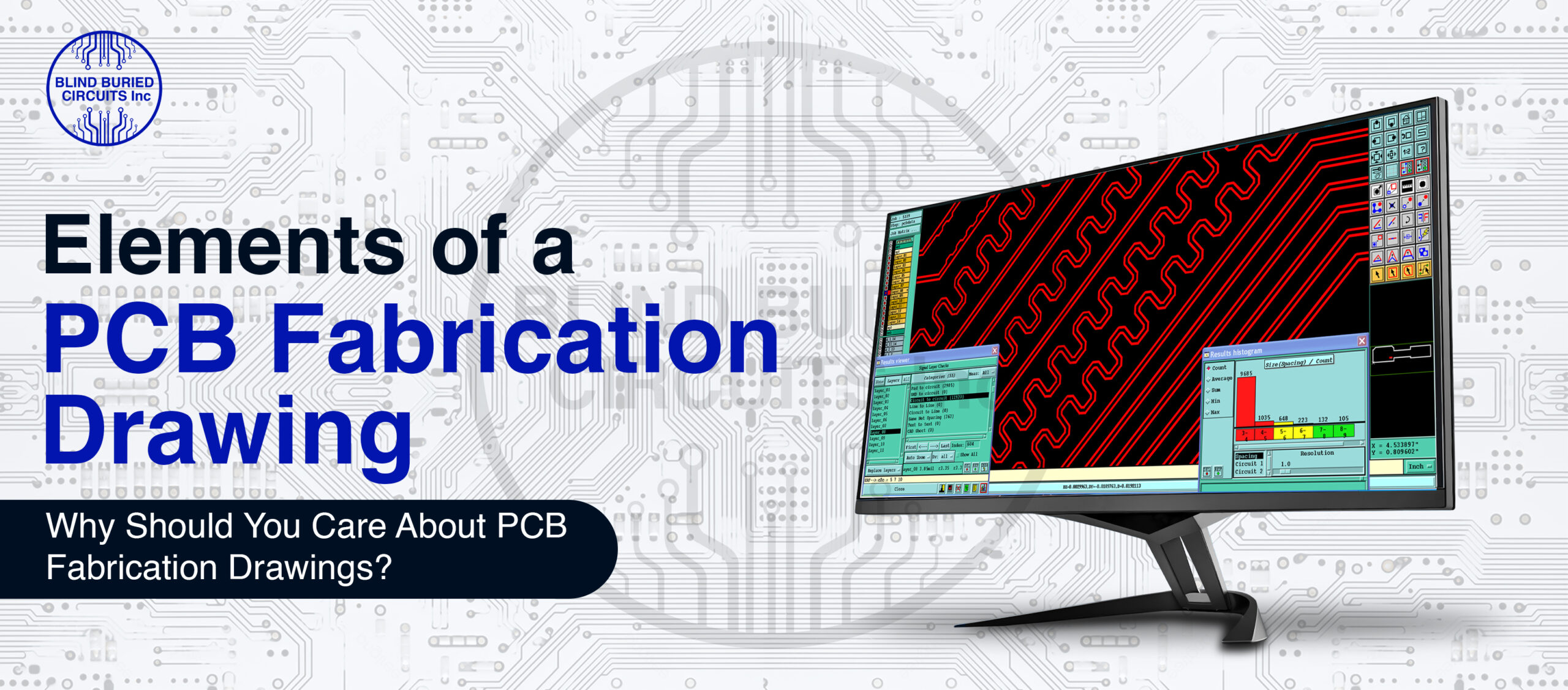
Step-by-Step Breakdown of a PCB Fabrication Drawing
A professional PCB fabrication drawing always follows a clear and structured format. Below are the important elements which manufacturers expect:
Title Block and Dimensioning
The title block includes the project name, part number, revision number, drawing scale, and approval signatures. Overall board size, cut-outs, and slot locations are specified here. Tolerances declare acceptable variation, ensuring mechanical compatibility during assembly.

Stack-Up Information
This section demonstrates the layer sequence, dielectric materials, copper thickness, and overall board thickness. A well-defined stack-up is crucial for impedance control,high-speed circuits and RF designs.

Drill Chart and Hole Details
A drill chart section lists plated and non-plated hole sizes, quantities, and tolerances. Because manufacturers rely on this to configure drilling machines accurately laser drilling in PCB fabrication ensures precise microvia formation minimizes misalignment, and enhances the overall reliability of multilayer PCBs.

Surface Finish & Plating Instructions
Common finishes include HASL, ENIG, or OSP. The drawing must clearly show which plating is required for pads, vias, and edge connectors because these details matter for solderability, durability, and overall performance.

Special Features (Impedance, Vias, Cut-outs)
Controlled impedance lines, blind or buried vias, and special routing notes fall under this section. Such specifications are vital for advanced electronics features mentioning RF, high-speed digital and aerospace applications.
If you’re planning custom pcb production or need fast pcb manufacturing, contact us at sales@blindburiedcircuits.com for more information.
Key Elements in Circuit Board Assembly Drawings
While a pcb fabrication drawing guides how to manufacture the bare board, a circuit board assembly drawing is important to guide correct placement of it with components.
The elements an assembly drawing includes:
- Reference designators and component outlines.
- Polarity indicators for diodes and capacitors.
- Placement notes and orientation guidelines.
- Soldering and inspection requirements.
Together, the pcb fab drawing and circuit board assembly drawing create a complete documentation package that eliminates ambiguity between design and manufacturing teams.
Ensuring Accuracy in PCB Fabrication: Best Practices
Accuracy in pcb fabrication directly impacts on product reliability. Even a minor negligence in the pcb fabrication drawing can literally cause a board to fail compliance or delay mass production. Here are some best practices:
- Use Design for Manufacturability (DFM): This validates that your design complies with the capabilities of the chosen manufacturer.
- Centralize Notes: Place all critical instructions in one section to avoid oversight.
- Preview Before Release: Cross-check Gerber files, stack-ups, and drill charts.
- Balance Speed and Quality: For fast pcb manufacturing, avoid overcomplicated features unless necessary.
Embedding precision into the drawing, you prevent rework, cost-effective, and makes sure that there is smoother custom pcb production.
Innovations & Trends in PCB Fabrication Drawings
By the method PCB fabrication drawings are being created is progressing rapidly, by advances engineering tools and digitalization.
However, key trends are as below:
Automation in Drawing Generation: modern CAD softwares can auto-generate standard notes, drill tables, and stack-up details, reducing manual errors.
AI and Machine Learning: AI tools now can scan PCB designs for common errors before releasing a pcb fab drawing to the manufacturer.
Integration with CAM: fabrication drawings are increasingly integrated directly with CAM software, by enabling manufacturers to simulate custom pcb production before going on to the physical processes.These innovations ensure that the process is faster, more reliable, and more scalable, especially for industries demanding fast pcb manufacturing.
These innovations ensure that the process is faster, more reliable, and more scalable, especially for industries demanding fast pcb manufacturing.
Practical Advice for Engineers and Designers
When preparing a pcb fabrication drawing,keep these practical tips in mind to ensure smooth manufacturing:
Choose the right tools: Leverage modern CAD packages simplify drawing preparation.
Avoid clutter: Keep drawings clean and avoid redundant data.
Think like a manufacturer: specify tolerances, surface finishes, and materials which aligns with available capabilities.
Communicate early: Share preliminary drawings with fabricators to confirm feasibility for advanced designs.
Avoid common mistakes: Don’t forget hole plating indicators, surface finish notes, or stack-up references.
Success in PCB manufacturing starts with accurate drawings. Blindburiedcircuit Inc offers hands-on support to ensure your designs are production-ready contact us now to get started.
Conclusion
A well-designed pcb fabrication drawing bridges the gap between design intent and manufacturing reality. By including crucial elements such as stack-up info, drill charts, material specs, and tolerances you enable smooth pcb fabrication and get rid of costly delays. Together with a circuit board assembly drawing, the pcb fab drawing forms the foundation of precise documentation.
Whether you’re pursuing fast pcb manufacturing for prototyping or large-scale custom pcb production, investing time in preparing accurate fabrication drawings will always be time saver, lower cost. The future promises even smarter documentation tools, but the principles of clarity, precise, and completeness remain timeless.


