Maintaining signal integrity is crucial in modern technology. If signals become distorted in any way, devices may malfunction. A problem most often associated with loss of signal quality is impedance. Impedance is simply how much a circuit impedes the smooth flow of electrical signals. In high-speed PCBs, measuring and controlling the impedance helps to ensure that signals are clean and strong.
This blog will cover the operation of 2-port shunt-through impedance measurement, its importance, and how it can help improve results with your PCB manufacturer or a PCB fabrication partner in the USA. We provide explanations and utilize short sentences to ensure everyone can follow easily.
What Is Impedance?
Impedance is a type of resistance that applies to changing or alternating signals and is very applicable to digital circuits. The low impedance definition describes when a circuit has a high ability to accept a signal and let it pass. In a PCB, you want the impedance to match what the circuit requires. If it does not comply, signals are bound to bounce back or die out.

Why is Impedance Important in Your PCB?
When creating a circuit board, ensuring your signals travel uninterrupted from one section to another is essential. If the impedance along the signal path changes too much, some of the signals may reflect. This phenomenon is known as signal reflection and can lead to errors, noise, or even complete device failure.
This is why impedance control is necessary in PCB design. Controlling the board design with regard to zones that require constant impedance ensures that there will be no abrupt changes within the conditions that matter most. With proper control, your circuit will be more dependable and faster.
How Do You Measure Impedance?
When checking if PCB traces meet specific impedance requirements, impedance testing is performed. There are multiple ways of doing this, but one notable and precise technique is the 2-port shunt-through impedance measurement.
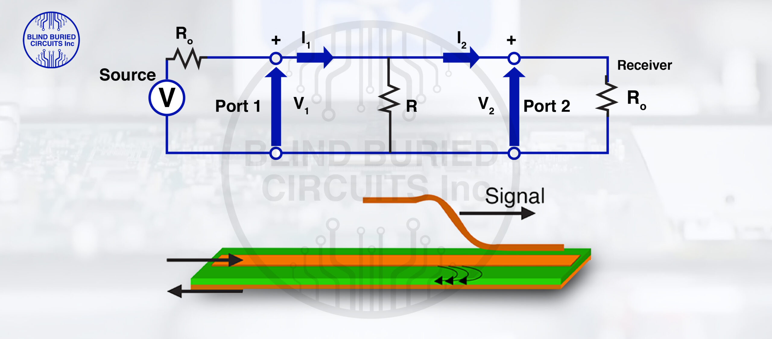
What Is 2-Port Shunt-Through Measurement?
This technique applies to PCBs with two test points (ports). One port is used to input a specific signal, and the other port outputs the signal after it has been processed. Meanwhile, the test configuration “shunts” or connects a defined resistor in the signal pathway and ground. The impedance of the trace can be determined by comparing the input and output.
This approach works great for low-impedance routes, which are often seen in power and ground connections. It also applies to high-speed signal lines.

Why 2-Port Shunt-Through Measurement?
Precision: This approach does low-impedance traces right, yielding accurate results.
Adapting to High-Speed Designs: This approach is particularly efficient for fast signals, where even slight changes in impedance can cause issues.
Assists with Problems: If your board has faults, this check can indicate areas where the impedance is inaccurate.
The Process of Impedance Testing for PCB Fabrication Companies
Through impedance testing, a PCB fabrication company or a PCB fabrication shop in the USA ensures that your board meets your specifications. Generally, the process follows:
- Examine Design: You specify the impedance requirements for certain traces, and the manufacturer works with them.
- Stackup Construction: The manufacturer selects materials and constructs the layers of the board to achieve the target impedance as suggested by the customer.
- Test Coupons: Every batch of the boards created includes accompanying small test pieces that undergo various tests, such as impedance testing.
- 2-Port Measurement: The shunt-through technique is employed to conduct measurements on the test coupons.
- Results Verification: The batch either passes or fails, depending on whether the impedance is correct or not; in this case, adjustments are made to the process.
What Impedance in a PCB is Affected By?
The following factors may affect impedance in your board:
- Trace Width: Wider traces result in lower impedance.
- Trace Thickness: Lower impedance is also achieved through thicker traces.
- Dielectric Material: The PCB’s layer influences the movement of signals across the board.
- Distance to Ground Plane: Traces that are nearer to the ground or power planes have lower impedance.
- Copper Weight: Changes in impedance can result from the use of heavier copper.
- Stack-up Design: The relationships between layers significantly influence impedance.
Best Practices Observed For Board Designing In Order To Control Impedance
To maintain your board’s signal integrity, observe the following guidelines:
1. Do Not Vary Trace Width
To maintain a steady impedance, refrain from changing the trace width along the length of the trace.
2. Do Not Use Sharp Turns in Trace Routing
Avoid points with sharp angles. Use smooth curves and 45-degree angles for turn bends.
3. Design Your Stackup Wisely
Design your stackup such that the placement of layers is optimal. Place the signal layers next to the ground and power planes.
4. Watch the Return Path
Provide fast and reliable return paths to the ground for high-speed signals. Ground planes must be sited near their corresponding signal traces.
5. Avoid Excessive Use of Vias
Impedance is affected every time a signal passes through a via (hole). The use of vias should, therefore, be kept to a minimum.
6. Choose the Right Materials
Select materials for the board that fit your signal requirements. Some materials outperform others for high-speed signals.
7. Communicate with Your Manufacturer
Make sure to inform your PCB manufacturing company of the impedance you require. Provide precise drawings and notes.
Manufacturing and Testing: What to Expect
If you place an order from a PCB manufacturer, the following process takes place:
- You provide impedance specs.
- They check your design and suggest changes if needed.
- They make test coupons for each batch.
- They use 2-port shunt-through or other impedance testing methods.
- You receive a report indicating whether your board meets the specifications.
If the impedance is off, the manufacturer may alter the board by changing the trace width, spacing, materials, or other factors to attempt retesting.
Why Is All This Important?
- Improved efficiency: Better-controlled impedance leads to reliable, high-speed circuits.
- Less Noise: Your device operates optimally when signals are kept clean and free from interference.
- Fewer Errors: Reduced signal reflection for miscalculation and data mistakes due to matching impedance systems.
- Simplified Problem-Solving: Within systems that utilize impedance testing, troubleshooting is simplified since problems can be easily located and corrected.
Key Points
| Step | What to Do | Why It Matters |
| Plan Impedance Early | Set specs in design stage | Avoid late changes, save money |
| Use Consistent Trace Width | No sudden changes | Keeps impedance steady |
| Choose Right Materials | Match material to signal needs | Better signal quality |
| Test with 2-Port Method | Accurate, reliable measurement | Find and fix problems early |
| Communicate with Manufacturer | Share clear drawings and needs | Fewer surprises, better results |
Final Thoughts
Impedance directly affects the integrity and quality of signal performance in PCBs. The 2-port shunt-through impedance measurement helps verify that the board performs as intended. Well-controlled impedance throughout the PCB’s design and manufacturing processes significantly reduces issues and enhances performance and customer satisfaction.
When engaging with a PCB manufacturing company or pcb fabrication USA partner, discuss your impedance requirements upfront. Obtain thorough testing and scrutinize the findings. This seemingly tedious step will improve your efficiency, reduce expenses, and relieve future stress.
For additional guidance on PCB design and manufacturing, maintain an inquisitive stance and continue learning. Excellent communication and meticulous planning yield superior results in project execution.


