When it comes to printed circuit boards, overall performance, cost, lead time and reliability gets 100% depending on the PCB stackup. The accurate arrangement of copper foils, insulating prepregs, core laminations and dielectric is more than just a design, it’s the way of defining the order, thickness and materials of each layer. A well-designed PCB board stackup, backed by clear documentation supports a solid stacking architecture to ensure the success from prototype to full-scale production. This blog explores the fundamentals of PCB layer stackup, key design considerations, and how manufacturers turn complex requirements into repeatable, reliable results.
This blog explores the fundamentals of PCB layer stackup, key design considerations, and how manufacturers turn complex requirements into repeatable, reliable results.
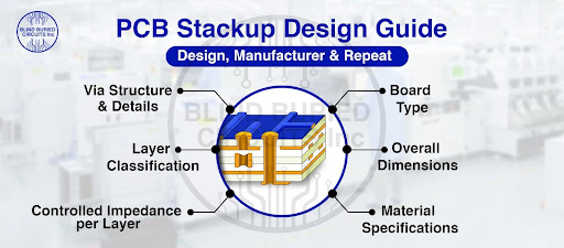
Understanding PCB Stackup Fundamentals
What’s PCB board stackup, PCB layer stackup, stackup plan & stacking architecture?
PCB board stackup – describes the overall construction of the PCB, including the materials, layer types, and total thickness. It covers FR-4 grade, copper thickness, dielectric material, and overall board thickness.

PCB layer stackup – PCB Layer Stackup shows the order and function of individual layers, not the full board it indicates which layer is for signal, ground, power, or silkscreen.

Stackup plan – it’s the design strategy for arranging layers to balance cost, signal integrity and reliability.

stacking architecture – This is most important to decide how to structure the complete stackup. it’s the chosen configuration style to define how layers and vias are organized in the PCB. A quick tip here: “Ensure to keep sequential arrangement for signal & plane layer’s in Multilayer stackup to avoid warpage issues” – Reach out to our sales engineer’s at sales@blindburiedcircuits.com if you want more tip’s or get any question resolved about stackup.
Benefits: signal integrity, EMI, cost efficiency
A strong PCB stackup delivers calculated impedance, reduces electromagnetic interference (EMI), and enhances thermal management. With a clear stackup plan, designers can optimize the number of layers to reduce cost while maintaining performance. A defined stacking architecture ensures repeatability in fabrication and avoids redesigns that delay production.
A well-planned stackup reduces EMI, improves signal integrity, and lowers cost.
Key Stackup Design Considerations
Material & layer thickness, impedance control, tolerances
The materials and layer thickness choice directly affects the PCB performance, factors such as dielectric constant, copper weight, and prepreg thickness determine signal quality and impedance. To keep up the consistency, manufacturers usually work within a ±10% impedance tolerance and critical tolerance of impedance as +/5%.. If you are looking to get your PCB layer stackup finalized then feel free to reach our sales engineer’s at sales@blindburiedcircuits.com for reliable performance and repeatability across your first prototype.
Avoiding common pitfalls in stackup design
Common issues in the PCB board stackup include copper imbalance, lack of symmetry and improper plane alignment for high-speed signals. However, these mistakes can cause warping or signal degradation.
A well-structured stackup plan cuts down these risks and speeds up approval during fabrication.
Why Manufacturing Partner Matters in PCB Projects
Communicating stackup details for custom PCB manufacturing
without communicating with the professional’s – even the best PCB Stackup can fail. Because for custom manufacturing, the fabricator does make arrangements in fudge factor and etch factor which does make change in line spacing or line width’s.For custom PCB manufacturing, designers should provide full stackup drawings, dielectric constants, desired material / substrate name or datasheet and target impedance values which clarifies that the manufacturer is building the stacking architecture exactly as intended. You can reach out to us for rigid, flex pcb & rigid flex standard or complex stackup requirements ar sales@blindburiedcircuits.com
How experienced PCB manufacturing partners reduce risk
A knowledgeable PCB manufacturing partner can anticipate fabrication challenges, recommend material alternatives to avoid supply delays, and advise on tolerance management. Their experience reduces risk and makes certain PCB board stackups perform consistently.
The best practice is to consider the turnkey contract manufacturer’s as they handle all part’s fabrication, parts & assembly labor which will matter for your project as turnkey manufacturer’s like “blindburiedcircuits Inc” performs all analysis (DFM & DFA) checks by keeping fabrication & assembly both in mind. Which helps the end customer to avoid any confusion’s with miscommunication or chasing more fabrication & assembly suppliers.
Implementing a Stackup: From Prototype to Mass Production
Using CAD tools for stackup drawing and simulation
Modern CAD tools simulate how a PCB layer stackup will perform under real-world conditions. These simulations test impedance, EMI, and thermal behavior against the defined stacking architecture. By validating the stackup plan digitally, teams reduce costly revisions and accelerate product launch.
Ensuring repeatability: design feedback loops with manufacturer
Repeatability is the key in electronics manufacturing. Creating structured feedback loops between design teams and fabricators helps capture real-world adjustments such as dielectric variations and incorporate them into the stackup plan. Once a PCB stackup is validated,the findings from prototype builds are captured in the documentation form and this process ensures it can be reproduced consistently at scale, to be integrated into the stackup plan.
Conclusion: From Design to Manufacturing and Repeatability
The PCB stackup is more than a structural detail; it is the foundation of performance, durability and cost-effectiveness. A conscientious engineer makes the precise stackup plan and clear stacking architecture, by minimizing the risk and which enables consistent, high-quality results.
Success depends on combining strong design practices with effective collaboration in PCB manufacturing. With the right approach, a PCB layer stackup becomes not only a technical necessity but also a competitive advantage ensuring every project can move smoothly from design, to manufacture, and repeat.
A thoughtfully engineered PCB layer stackup isn’t just about today’s design but it’s an investment in long-term reliability, manufacturability, and success.


