Printed circuit boards (PCBs) are the backbone of modern electronics, from advanced medical devices to automotive systems and aerospace technology. Copper wrap plating, a most important process, comes when there are plated via’s to be used in double sided or multilayer pcb’s. As this strengthens the connections, improves conductivity, and enhances the overall longevity of the interconnections.
To ensure the consistent high quality performance in the PCB assemblies, the pcb copper plating process must be carefully controlled. Factors like optimal copper plating thickness directly influence conductivity and long term reliability.
Understanding PCB Copper Plating Thickness in Modern Electronics
Why Copper Plating Thickness Matters on surface & Via’s in PCB Design
The PCB copper plating thickness matters in PCB design directly: depending on the current requirement, how well it dissipates heat, and how mechanically strong it will be. In the applications of various PCB materials, the copper thickness plays a vital role in defining performance, especially for thermal and electrical efficiency. Whereas, standard industry copper thickness is 1oz as most of the core’s (having dielectric & copper) are available with the 1oz copper thickness. Wondering to know max & minimum copper thickness we can achieve, then request our capabilities by email us at sales@blindburiedcircuits.com
An important information for pcb designer’s is that, If the copper requirement’s & plating is too thick, this can elevate the cost so the right step is to get stackup cross check and finalize as per requirement by sharing it to your trusted PCB manufacturer.
Carefully controlling the copper thickness is critical for high-frequency designs like RF modules and advanced communication systems. The accuracy is essential for minimizing signal loss and maintaining the stable impedance.
Industry Standards for PCB Copper Plating Thickness (H3)
The organizations such as IPC defines accepted ranges for plating thickness, as by following IPC-6012B guidelines it ensures that copper wrap plating around vias and through-holes offers the reliable mechanical strength.
As for the industries like aerospace, medical and defense, the requirements of strict criteria often calls for IPC CLASS III and specialized processes. Our certifications such as IPC A 600 & 610 qualified team, ISO 13485 & ISO 9001 Certified team become essential in proving compliance and quality control.

The PCB Copper Plating Process Explained
Step-by-Step Breakdown of the PCB Copper Plating Process
The PCB copper plating process is cautiously regulated to ensure constancy and performance:
- Surface Cleaning – Preparing the board by removing impurities.
- Electrolytic Plating – Depositing copper evenly across traces and vias.
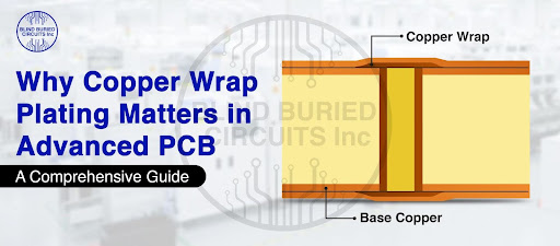
- Copper Wrap Plating – Extending copper around via edges to strengthen connections.
- Protective Finishes – Applying ENIG, HASL, or other finishes for oxidation resistance.
Each stage is critical, as even the slightest deviations in plating can affect copper plating conductivity in PCB designs outcomes.

Quality Control Measures in PCB Copper Plating
The PCB manufacturer (blindburiedcircuit’s Inc) follows the strict inspection methods to verify plating thickness and adhesion. Our ISO 9001 certification assures process consistency, while IPC A 600 & IPC A 610 visual inspections provides validation of acceptable criteria for manufactured electronics.
We make sure that our boards are not only reliable but also environmentally responsible by compliance and safety with UL 94-V requirements and RoHS compliance and this gives the confidence to provide quality assurance. .
Thermal Management Benefits of Proper Copper Plating
Apart from electrical properties, copper surface thickness & plating improves thermal dissipation. as while doing troubleshooting of assembled pcb there are good chances of heat generated by the high-power components must spread evenly across the board. Competent plating thickness helps avoid hot spots which extends product lifespan in demanding environments like EV chargers or industrial controls.
A smart way to dissipate the high power IC’s/ connector’s is the thermal Via’s placement works as heatsink to dissipate the heat to the plane layers on to the internal layer’s of PCB.
PCB Board Assembly Manufacturing and Copper Plating
How Wrap Copper Plating helps in PCB Board Assembly Manufacturing
During soldering and reflow, plated vias remain high levels of thermal stress. If the PCB copper plating thickness is deficient, vias may crack or separate, causing reliability issues. Due to which the Wrap plating is performed during Via’s plating process to ensure no crack found due to thermal stress.
Role of Custom PCB Production in Achieving Precision Plating
Every project is different and special for end customer, which makes custom PCB production so worthwhile. By implementing plating parameters to the application, manufacturers can balance longevity, cost, and performance. Get your custom design review and quoted by our expert sales & engineering team by emailing on sales@blindburiedcircuits.com
Conclusion: Driving Innovation with Copper Wrap Plating in PCBs
Copper wrap plating plays a vital role in building trustable, high-performance boards. Factors such as PCB copper plating thickness and parameter’s, a carefully managed PCB copper plating process for Vias, and strong copper plating conductivity in PCB applications together to ensure that the products meet both performance and safety standards
By coalition with certified partners, businesses can confidently bring the next generation of innovative electronic products to market. Feel free to contact our sales or engineering team for your design heavy copper requirement’s for quick feedback & quotation.


