Objective
Many flexible PCB failures originate long before testing begins. Material selection determines how well a flex circuit survives bending, soldering, vibration, moisture exposure, and long-term field use. A design may pass electrical verification yet still experience copper fatigue, coverlay damage, or reduced service life if even a single wrong material stack-up is chosen. This guide explains how to select flexible PCB materials based on bend requirements, signal performance, thermal conditions, manufacturability, and reliability objectives.
Key Takeaways
- Match the material to the way the circuit will bend.
- Use polyimide for many reliable flex circuit materials.
- Consider LCP or PTFE for RF and high-speed signal needs.
- Use RA copper when repeated bending is expected.
- Use adhesiveless laminates when thinness, fine lines, or bend life matter.
- Keep a multilayer flex PCB thin and simple in bend areas.
- Add stiffeners only where support is needed.
- Review DFM rules before the stack-up is finalized.
- Avoid choosing flexible PCB materials based on cost alone.
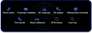
Table Of Contents
- Why Flexible PCB Materials Matter
- Static Bend Vs Dynamic Bend
- Common Flex Circuit Materials
- Flexible PCB Material Selection by Application
- Copper Choices For Flex PCB Material Selection
- Adhesive Vs Adhesiveless Laminates
- Coverlay, Stiffeners, And Shielding
- Multilayer Flex PCB Material Selection
- DFM Considerations for Flexible PCB Materials
- Common Failure Modes Caused by Incorrect Material Selection
- Common Flexible PCB Material Selection Mistakes
- Material Selection Checklist
- Industry Standards For Flex PCB Design
- FAQs
- Conclusion
Why Flexible PCB Materials Matter
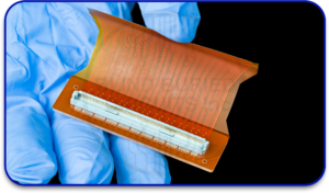
A flex PCB is not just a soft rigid board. It must carry power and signals while it bends, folds, or fits into a small space.
That is why material selection should be finalized before layout starts. A circuit can look correct on screen and still fail if the stack is too thick, too stiff, or wrong for the bend. The right stack helps the circuit survive handling, assembly heat, vibration, moisture, and movement. The wrong stack can lead to cracked copper, lifted coverlay, delamination, signal loss, or short service life.
Material choice also affects cost. Some materials are cheaper at the start but may increase risk during assembly or field use. A low-cost material may not save money if it causes rework, failed testing, warranty issues, or redesign later.
Good flex PCB material selection is not only about choosing a base film. It is about matching the full stack-up to the application. Base film, copper type, adhesive system, coverlay, stiffener, shielding, and thickness all affect how the circuit performs in real use.
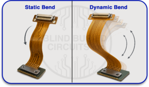
Static Bend Vs Dynamic Bend
Good material selection starts with understanding the bend type.
A static flex circuit bends during installation and then stays in place. This is common in cameras, displays, sensors, and compact assemblies.
A dynamic flex circuit bends many times during use. This is common in hinges, printers, foldable devices, robotics, medical tools, and wearables.
Bend radius is one of the most important factors in flex reliability. As a general guideline, static flex circuits often use a minimum bend radius of approximately 6–10 times the flex thickness, while dynamic flex applications may require 10–20 times the thickness or more depending on copper weight, layer count, and expected bend cycles.
Bend areas require special routing rules and should not be treated the same as rigid PCB routing regions. Trace geometry, copper distribution, and stack-up design must be optimized to reduce mechanical stress during flexing.
Common Flex Circuit Materials
Most flex circuit materials include a base film, copper foil, bonding layer, coverlay, and sometimes a stiffener or shield.
| Material Area | Common Choice | Main Use |
| Base Film | Polyimide | Heat resistance and flexibility |
| Low-Cost Film | PET | Simple static circuits |
| High-Frequency Film | LCP Or PTFE | RF and high-speed signals |
| Copper Foil | RA Or ED Copper | Conductive traces |
| Protection Layer | Polyimide Coverlay | Trace protection |
| Support Layer | FR-4, PI, Or Metal | Connector support |
Polyimide Flexible PCB Materials
Polyimide is the most common base film for quality flexible PCB materials. Polyimide offers excellent thermal stability and can withstand standard SMT assembly and reflow soldering processes while maintaining mechanical integrity.
It also stays stable in demanding environments.
Polyimide is a good choice for industrial, medical, automotive, aerospace, and consumer products. It works well when the circuit must be thin, light, and reliable.
PET Flex Circuit Materials
PET, also called polyester, is usually used for simple and lower-cost circuits. It can work in keypads, printed sensors, labels, and static circuits.
PET is not a strong choice for high heat, hard bending, or most soldered assemblies. Use it only when the application is simple, and the limits are clear.
LCP And PTFE For High-Speed Designs
LCP and PTFE are selected when low dielectric loss, controlled impedance, and stable RF performance are required. Their electrical properties make them suitable for microwave, mmWave, antenna, and other high-frequency applications. They help in RF, microwave, antenna, radar, telecom, and high-speed digital designs.
LCP also has extremely low moisture absorption compared with many other flex substrate materials. This helps maintain stable dielectric properties and signal performance in humid environments and outdoor applications.
For impedance-controlled flex circuits, dielectric thickness, material consistency, and copper surface profile should be reviewed early in the design process to help achieve reliable signal integrity targets.
Flexible PCB Material Selection by Application
Different applications place different stress on flexible PCB materials. A circuit used once during installation does not need the same material stack as a hinge circuit that bends thousands or millions of times. A low-speed sensor flex also has different needs from an RF antenna or high-speed digital flex circuit.
The table below gives a practical starting point for flex PCB material selection by application.
| Application | Common Material Choice | Why It Works | Key Design Note |
| Static bend circuits | Polyimide with ED or RA copper | Works well where the bend happens during installation and then stays fixed | Keep the bend radius suitable for the final stack thickness |
| Dynamic bend circuits | Polyimide with RA copper and adhesiveless laminate | Better bend life and improved resistance to copper fatigue | Avoid thick copper, stacked vias, and stiff areas in the bend zone |
| Low-cost static circuits | PET or polyester-based material | Suitable for simple circuits with limited heat and movement | Avoid high-temperature soldering and repeated flexing |
| High-speed digital circuits | Polyimide, LCP, or PTFE depending on signal needs | Helps support impedance control and lower signal loss | Review dielectric thickness, copper roughness, and stack-up early |
| RF and antenna circuits | LCP or PTFE | Low loss and stable dielectric performance at higher frequencies | Confirm dielectric properties and impedance targets before layout |
| Medical or wearable devices | Thin polyimide with suitable coverlay | Offers flexibility, reliability, and compact packaging | Consider bend cycles, skin contact environment, moisture, and handling |
| Automotive or industrial flex circuits | Polyimide with proper coverlay and stiffeners | Handles heat, vibration, and assembly stress better than low-cost films | Match material to temperature, vibration, and connector support needs |
| Multilayer flex PCB | Polyimide-based multilayer stack-up | Supports higher routing density, shielding, and controlled impedance | Keep bend areas thin and avoid unnecessary layers in flex regions |
| Connector or component support areas | FR-4, polyimide, stainless steel, or aluminum stiffeners | Adds local support where bending is not wanted | Do not place stiffener edges directly on bend lines |
| EMI-sensitive circuits | Copper shielding, conductive ink, or EMI shielding film | Helps reduce noise and protect sensitive signals | Balance shielding performance with flexibility and thickness |
This table should be treated as a practical guide, not a fixed rule. Final material selection should always consider bend radius, bend cycles, assembly process, operating temperature, current load, impedance needs, and manufacturing capability.
Copper Choices For Flex PCB Material Selection
Copper choice affects electrical performance and bend life.
Rolled annealed copper, often called RA copper, has traditionally been preferred for dynamic flex applications because of its higher ductility and improved resistance to bending fatigue.
Electrodeposited copper, often called ED copper, is common in standard or static flex designs. It can be cost-effective, but it is not always best for repeated movement.
Copper thickness matters too. Thicker copper can carry more current, but it makes the flex area harder to bend. Heavy copper may also need a larger bend radius.
For high-speed flex circuits, copper surface roughness should also be checked. Lower-profile copper can reduce conductor roughness losses at high frequencies, helping preserve signal integrity in high-speed digital and RF circuits.
Some high-ductility ED copper grades can also perform well in flex applications, but RA copper remains a common choice when maximum bend life is required.
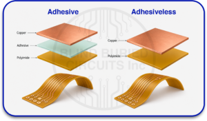
Adhesive Vs Adhesiveless Laminates
Flex laminates can use adhesive-based or adhesiveless constructions.
Adhesive-based laminates use acrylic or epoxy adhesive to bond copper to the base film. They are common and can work well for many standard circuits.
Adhesiveless laminates eliminate the separate adhesive layer between copper and polyimide, resulting in improved dimensional stability, reduced thickness, and enhanced flex-life performance.
Adhesiveless material can cost more at the start. It may still be the better choice when failure risk, thickness, or long-term movement matters. Blind Buried Circuits can help review this choice before the stack-up is finalized.
Coverlay, Stiffeners, And Shielding
Coverlay protects copper traces from handling, dust, moisture, and mechanical stress. Polyimide coverlay is often used because it bends well and handles heat.
Polyimide coverlay is generally preferred in dynamic bend regions because it provides superior mechanical durability compared with flexible solder mask.
Stiffeners are used where the circuit should not bend. They support connectors, contact fingers, components, and solder joints. Common stiffener materials include FR-4, polyimide, stainless steel, and aluminum.
A stiffener edge should not sit directly on a bend line. That can create a hard stress point. Over time, this stress can lead to copper cracks or coverlay damage.
Shielding may be needed when signals are sensitive. Options can include copper, conductive ink, or EMI shielding film. The right choice depends on signal type, space, cost, and flexibility needs.
Multilayer Flex PCB Material Selection
A multilayer flex PCB helps when the design needs more routing, controlled impedance, shielding, or separate power and ground layers.
It also becomes thicker and stiffer than a single-layer or double-layer flex circuit. Material decisions should be finalized early in the design process and before layout release. Stack-up decisions influence routing density, bend performance, impedance control, and long-term reliability.
Keep the bend area simple. Avoid heavy copper, sharp corners, stacked vias, and extra layers in the bend zone.
Use gradual curves instead of sharp trace turns. Keep traces smooth through the bend. Review the stack-up early so copper is placed where strain is lower.
A multilayer flex PCB should not be chosen only because the layout is crowded. First check whether routing can be simplified, connectors can be moved, or the bend area can stay thinner.
DFM Considerations for Flexible PCB Materials
Design for manufacturability should be reviewed before flexible PCB materials are approved. A material stack may look suitable from a performance point of view, but it also needs to be practical for fabrication, assembly, inspection, and long-term use.
The first DFM concern is total stack thickness. A thicker stack reduces flexibility and increases strain during bending. This becomes even more important in dynamic bend applications. Designers should keep bend zones as thin as possible and avoid adding unnecessary copper, adhesive, shielding, or stiffener material in areas that must flex.
The second concern is copper distribution. Uneven copper can create stress imbalance during bending and fabrication. Wide copper pours, heavy planes, and sudden copper transitions can make one area stiffer than another. In flex regions, copper should be distributed carefully, and traces should follow smooth paths instead of sharp corners.
The third concern is via placement. Vias should generally be kept out of active bend areas. A via adds stiffness and can become a stress concentration point. In multilayer flex PCB designs, stacked vias, dense via fields, and plated holes near bend regions should be reviewed carefully with the manufacturer.
Coverlay design also needs attention. Coverlay openings should be sized properly for pads and assembly needs. Poorly planned openings can create weak edges, soldering issues, or exposed copper. The coverlay adhesive system must also match the bend requirement and the assembly process.
Stiffener placement is another key DFM point. Stiffeners are useful, but they must be placed with care. A stiffener should support connectors, components, or contact areas without forcing a hard transition directly at the bend line. Smooth transition areas help reduce stress.
For high-speed and RF flex circuits, DFM also includes impedance control, dielectric consistency, copper roughness, and material tolerance. These details should be discussed before layout is locked. Changing material after routing can affect impedance, thickness, bend radius, and final performance.
Good DFM review helps prevent avoidable issues before production. It also helps align material choice with actual fabrication capability, not just design intent.
Common Failure Modes Caused by Incorrect Material Selection
Incorrect material selection can create failures that may not appear during basic electrical testing. Some problems only show up after assembly, bending, temperature cycling, vibration, or field use.
One common failure mode is copper cracking. This often happens when the copper is too thick, the bend radius is too tight, or the wrong copper type is used for repeated movement. Dynamic flex circuits are especially sensitive to copper fatigue.
Another common issue is delamination. This can happen when the adhesive system, base material, or laminate construction is not suitable for heat, moisture, bending, or assembly stress. Delamination can weaken the circuit and may lead to open circuits or insulation problems.
Coverlay lifting is also a material-related risk. If the coverlay adhesive does not match the application or if the bend zone is too tight, the coverlay may separate from the flex surface. This can expose traces and reduce mechanical protection.
Signal loss can occur when high-speed or RF designs use the wrong dielectric material, poor copper surface profile, or inconsistent stack-up thickness. A circuit may still pass basic continuity checks but fail to deliver stable signal performance in real operation.
Solder joint damage can happen when components are placed too close to bend areas or when stiffeners are not used correctly. A flexible circuit should bend where it is designed to bend, not at solder joints, connectors, or component pads.
Moisture-related instability is another concern. Some materials absorb more moisture than others. In high-frequency, outdoor, or humid environments, moisture can affect dielectric properties, signal behavior, and long-term reliability.
These failures show why flex PCB material selection should be reviewed early. The goal is not only to make the circuit work on day one, but to help it survive the environment and movement it will face in use.
Common Flexible PCB Material Selection Mistakes
Many flex circuit problems come from simple material selection mistakes. These mistakes are often made when the design team treats a flex PCB like a thin rigid PCB.
The first mistake is choosing material based only on cost. Low-cost material may be acceptable for simple static circuits, but it can be risky for high-heat, high-bend, or high-reliability applications. A cheaper stack-up can become expensive if it causes failure, redesign, or production delay.
The second mistake is using the same material stack for static and dynamic applications. A circuit that bends once during installation has very different needs from a circuit that bends repeatedly during operation. Dynamic flex designs usually need better bend-life planning, suitable copper, thinner stack-ups, and careful routing.
The third mistake is ignoring copper thickness. Thick copper may be needed for current carrying, but it also increases stiffness. If heavy copper is placed in a bend zone, it may reduce flexibility and increase the risk of cracking.
The fourth mistake is adding too many layers in bend areas. A multilayer flex PCB can solve routing problems, but it can also make the circuit harder to bend. Bend zones should stay as simple and thin as possible.
The fifth mistake is placing stiffener edges too close to bend lines. Stiffeners are helpful in connector and component areas, but poor placement can create a hard stress point. This may lead to copper fatigue or coverlay damage.
The sixth mistake is choosing flexible solder mask where polyimide coverlay would perform better. Flexible solder mask may work in some cases, but polyimide coverlay is often stronger for dynamic bending and demanding environments.
The seventh mistake is waiting too long to involve the manufacturer. Flex PCB material choices affect fabrication, assembly, bend reliability, and cost. If the manufacturer reviews the stack-up too late, the design may need changes after layout is already complete.
Avoiding these mistakes helps reduce risk and keeps the flex circuit more manufacturable, reliable, and suitable for its real application.
Material Selection Checklist
Use this checklist before approving the stack-up and material set:
Will the circuit bend once or many times?
What bend radius is available?
How many bend cycles are expected?
What temperature will the circuit face?
Will the board go through reflow soldering?
Does the design need RF or high-speed performance?
How much current must the copper carry?
Is EMI shielding needed?
Where are connectors and components placed?
Can the bend area be made thinner?
Has the manufacturer reviewed the stack-up?
This checklist helps avoid material choices based only on price. It also helps catch bend, heat, and stack-up problems before production.
Industry Standards For Flex PCB Design
Industry standards such as IPC-2223, Sectional Design Standard for Flexible Printed Boards, and IPC-6013, Qualification and Performance Specification for Flexible Printed Boards, provide guidance for material selection, bend requirements, manufacturing quality, and reliability expectations.
Designers working on critical applications should review these standards alongside manufacturer recommendations.
Standards are useful because they give a common reference point for design, fabrication, inspection, and performance expectations. They do not replace application-specific review, but they help teams avoid guesswork when choosing flex circuit materials and stack-up details.
Conclusion
Selecting the right materials is critical to the performance and reliability of any flex circuit. Factors such as bend requirements, operating temperature, signal integrity, assembly processes, and mechanical constraints should all be considered early in the design phase.
Whether the application requires a simple single-layer design or a more complex multilayer flex PCB, the stack-up should be chosen based on real-world performance requirements rather than cost alone. Careful evaluation of base films, copper types, laminate construction, coverlay, and support materials can help prevent failures, improve manufacturability, and extend product life.
By reviewing material requirements before the layout is finalized, design teams can reduce risk, avoid costly revisions, and achieve a more reliable end product. A well-planned material strategy supports both manufacturing efficiency and long-term field performance.
FAQs
What Are The Best Flexible PCB Materials For Most Products?
Polyimide, copper foil, and polyimide coverlay are common choices for many reliable flex designs. They offer heat resistance, bend performance, and stability.
What Is The Difference Between RA Copper And ED Copper?
RA copper is usually better for repeated bending. ED copper is often used in standard or static flex circuits where movement is limited.
When Should I Use Adhesiveless Laminates?
Use adhesiveless materials when the design needs a thinner stack, fine lines, better bend life, or stronger thermal performance.
Is PET A Good Flex PCB Material?
PET can work for simple, low-cost, static circuits. It is not ideal for high heat, repeated bending, or demanding assemblies.
What Material Is Best For High-Frequency Flex Circuits?
LCP and PTFE are common choices for high-frequency and RF flex circuits. They help control signal loss and moisture-related changes.
Can A Multilayer Flex PCB Bend Safely?
Yes, but it needs careful design. It is thicker, so the bend radius must be larger and the bend area should stay simple.
Why Does Copper Thickness Matter In Flexible PCB Materials?
Increasing copper thickness improves current-carrying capacity but also increases stiffness and strain during bending. Dynamic flex applications typically benefit from thinner copper to maximize bend life.
Why Does Coverlay Matter In Flex PCB Material Selection?
Coverlay protects copper traces and insulation. It helps the circuit survive bending, handling, dust, and moisture.


