Objective
This blog explains how PCB vias help different layers of a circuit board connect. It is written for readers who want a simple but correct understanding of multilayer circuit boards. Blind Buried Circuits works with multilayer and HDI PCB designs where via planning affects routing density, manufacturing complexity, signal integrity, reliability, and overall cost.
Key Takeaways
- Most vias structures are plated holes that create electrical connections between copper layers.
- Through-hole vias pass through the full board.
- Blind vias connect an outside layer to an inside layer.
- Buried vias connect inside layers only.
- HDI PCB structures help route small and dense boards.
- Good via design improves reliability and manufacturability.
- Poor via planning can cause signal, plating, soldering, and cost issues.
Table Of Contents
- What PCB Vias Are
- Why Vias Matter
- Main Types Of Vias
- How PCB Vias Are Made
- HDI Vias Structures And Microvias
- Via Design Rules That Matter
- Common PCB Via Failure Modes And Reliability Issues
- Common Problems
- FAQs
What PCB Vias Are
A printed circuit board has copper paths called traces. These traces carry signals, power, and ground between parts.
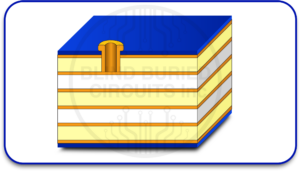
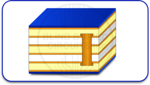
In simple boards, copper may sit on one or two sides. In multilayer circuit boards, copper also sits inside the board. Those inside layers are hidden after the board is pressed together.
These vias connect the layers. A via is a small drilled hole with copper plated on the inside wall. That copper lining creates an electrical path from one layer to another.
A via functions as a vertical electrical interconnect between conductive layers within the PCB stack-up. A signal can enter the tunnel from one copper layer and come out on another layer.
This makes the board easier to route. It also helps designers use inner layers for power, ground, and signal control.
Why Vias Matter in Modern PCB Design
Modern electronics are small. They also need more parts, more signals, and better performance.
That is why multilayer vias matter. They allow a circuit to move between layers without taking up too much surface space.
A board may need vias when it has:
- Small chips with many pins
- Dense connectors
- High-speed signals
- Power and ground planes
- Limited board space
- Signals that must avoid crossing each other
- Components on both sides of the board
Vias also allow controlled transitions between signal layers while maintaining access to nearby reference planes for signal return paths.
Without vias, many multilayer circuit boards would be too large or too crowded. Vias help keep the layout cleaner and more practical.
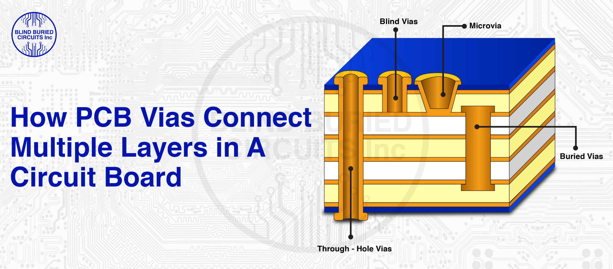
Main Types Of Vias
Not every via does the same job. The correct via type depends on the layers that need to connect.
| Via Type | What It Connects | Where It Is Used |
| Through-Hole Via | Top layer to bottom layer | Standard boards |
| Blind Via | Outer layer to inner layer | Dense routing |
| Buried Via | Inner layer to inner layer | Advanced multilayer boards |
| Microvia | Short, small layer connection | HDI boards |
| Via-In-Pad | Via placed inside a pad | Fine-pitch parts |
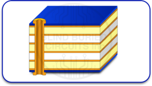
Through-Hole Vias
A through-hole via goes through the full board. It starts on the top layer and ends on the bottom layer.
This is the most common via type. It is cost-effective, mechanically robust, and supported by virtually all PCB fabrication processes.
The main downside is space. A through-hole via passes through every layer, even if it only needs to connect two of them. This can block routing room on other layers.
Blind Multilayer Vias
A blind via starts on the top or bottom surface and stops at an inner layer. It does not pass through the full board.
Blind vias improve routing density by freeing inner-layer routing channels that would otherwise be occupied by through-hole vias. They are useful under fine-pitch parts, such as BGAs and compact connectors.
They also add process steps. This can increase cost compared with simple through-hole vias.
Buried Multilayer Vias
A buried via connects internal layers only. It cannot be seen from the outside of the finished board.
Buried vias are useful when inner layers need direct connections without using surface space. They are common in advanced multilayer circuit boards. Buried vias generally require sequential lamination processes, increasing fabrication complexity and cost.
How PCB Vias Are Made
The basic PCB manufacturing process for vias starts with drilling. A machine drills holes in the board at the via locations.
The hole walls are then cleaned. After that, copper is deposited and plated inside the holes. This plating turns the empty hole into a working electrical connection.
For through-hole vias, the process is usually more direct. The full board is laminated first. Then the holes are drilled and plated.
For blind and buried vias, the process can be more complex. Some vias must be made before the full board is pressed together. This is why blind and buried via boards need a clear stack-up before manufacturing starts.
A stack-up shows the order of copper layers, insulating layers, and materials in the board. It also shows which layers each via must connect.
At this stage, Blind Buried Circuits can review whether the via structure fits the board design, layer count, and build method.
HDI Via Structures And Microvias
HDI means high-density interconnect. HDI vias are used when a circuit needs many connections in a small area.
Microvias are very small blind vias. They are usually made with a laser instead of a mechanical drill. A microvia typically connects one layer to an adjacent layer and is commonly used in HDI designs with sequential lamination.
These are common in phones, medical devices, wearables, cameras, sensors, and compact industrial products.
They help designers:
- Save board space
- Route fine-pitch chips
- Shorten some signal paths
- Reduce large through-hole via use
- Improve dense layer connections
Microvias still need careful planning. A poorly designed microvia can have weak plating at the bottom. Industry reliability studies generally favor staggered microvias over stacked microvias when routing constraints allow, because stress concentration can increase at stacked microvia interfaces.
Via Design Rules That Matter
Good vias are not only about hole placement. Several small details affect quality.
Annular Ring
The annular ring is the copper area around the drilled hole. It gives the drill a safe landing area.
If the annular ring is too small, drilling movement can reduce the copper connection. This may cause weak vias or open circuits.
Aspect Ratio
Aspect ratio compares board thickness to hole diameter. A thick board with a tiny hole is harder to plate well. Microvias are typically designed with low aspect ratios to help ensure reliable copper plating. Fabricators often specify maximum aspect-ratio limits for laser-drilled microvias.
Higher aspect ratios make uniform copper deposition more difficult, increasing the risk of thin plating regions that may reduce long-term via reliability. That can reduce via reliability, especially in thicker multilayer circuit boards.
Via Stub
A via stub is the unused part of a via that extends beyond the layer where the signal ends.
In low-speed boards, this may not matter much. In high-speed and high-frequency designs, via stubs can create impedance discontinuities and resonant effects that degrade signal integrity. Back drilling is commonly used on high-speed backplanes, networking equipment, and other designs where long via stubs could affect performance.
Via-In-Pad
Via-in-pad means the via is placed inside a component pad. This is common under small BGA parts.
An open via-in-pad can pull solder into the via during assembly. IPC-4761 filled and capped via structures are commonly used to prevent solder wicking and improve assembly reliability. They must be specified clearly in the fabrication notes.
Thermal And Power Needs
Some vias carry heat or current. A single small via may not be enough.
Thermal via arrays are commonly placed beneath power devices and heat-generating components to improve heat transfer into internal or external copper planes.
Return Path Considerations
When a signal changes layers through a via, its return current must also find a continuous path through nearby reference planes. If the return path is interrupted, signal integrity and EMI performance may suffer. High-speed PCB designs often use stitching vias near signal-layer transitions to maintain a low-impedance return path.
Common PCB Via Failure Modes And Reliability Issues
PCB via failures often happen when the via structure, board thickness, plating quality, thermal stress, or assembly process is not planned correctly. A via may look small, but it has to survive drilling, plating, lamination, soldering, heat cycling, vibration, and long-term electrical use.
One common issue is weak or uneven copper plating inside the via barrel. If the plating is too thin, the via may crack during thermal cycling or fail after repeated heating and cooling. This is especially important in multilayer circuit boards where vias pass through several material layers.
Barrel cracking is another reliability concern. It can happen when the board expands and contracts during operation or assembly. The copper inside the via and the surrounding laminate may expand at different rates, creating stress over time.
Microvias can also fail when they are poorly designed or stacked without enough reliability review. Weak plating at the base of a microvia, poor laser drilling, or stress between stacked microvia interfaces can lead to open circuits.
Via-in-pad issues are also common. If the via is not filled and capped properly, solder may flow into the hole during assembly. This can reduce solder volume on the component pad and create weak solder joints.
High-speed boards may face signal reliability problems from long via stubs, poor reference-plane transitions, or missing stitching vias. These issues may not break the circuit physically, but they can affect signal quality, timing, EMI behavior, and overall board performance.
Good via reliability starts with proper stack-up planning, realistic aspect ratios, suitable via type selection, correct plating requirements, and early review with the PCB manufacturer.
Common Problems
Via problems often start with small design choices.
Common issues include:
- Weak copper plating inside the hole
- Small annular rings
- Drilling misalignment
- Cracks from heat cycling
- Solder loss through open via-in-pad
- High-speed signal loss from via stubs
- Extra cost from unnecessary blind or buried vias
- Poor stack-up planning before fabrication
- Barrel cracking caused by thermal cycling and coefficient-of-expansion mismatch
These problems are easier to prevent before production. Once the board is fabricated, via issues can be hard to fix.
A good design review checks which vias are required, which vias are too costly, and which vias may affect performance.
Industry Standards For PCB Via Design
Standards such as IPC-2221, IPC-2226, IPC-6012, and IPC-6016 provide guidance for via design, fabrication quality, HDI structures, and reliability requirements. Designers should review these standards alongside fabricator capabilities during stack-up planning.
Conclusion
Vias are fundamental electrical interconnect structures that enable modern multilayer, HDI, and high-speed board designs. They allow signals, power, and ground to move efficiently throughout the stack-up while supporting increasingly complex routing requirements.
The right via structure depends on layer count, signal performance, component density, current requirements, manufacturing constraints, and budget. Through-hole designs remain a reliable option for many applications, while blind, buried, and microvia technologies help support advanced routing strategies in compact electronics.
Careful planning early in the design process helps improve manufacturability, reliability, and overall board performance.
Blind Buried Circuits helps teams review via structures before production so the board can be built with fewer delays and fewer surprises.
FAQs
What Are PCB Vias?
PCB vias are small plated holes that connect copper layers inside a circuit board. They allow signals, power, and ground to move from one layer to another.
Why Are Multilayer PCB Vias Important?
Multilayer vias allow different layers to work together. They help route complex designs without making the board too large.
What Is The Difference Between Blind And Buried Vias?
A blind via connects an outside layer to an inside layer. A buried via connects only inside layers and is not visible on the board surface.
When Are HDI PCB Vias Needed?
HDI vias are used when the board has very small parts, tight routing space, or dense layer connections. They are common in compact electronic products.
Do Vias Affect Signal Quality?
Yes. Via geometry, stub length, antipad design, reference-plane transitions, and placement can significantly affect signal integrity in high-speed designs.
Why Does Via Plating Matter?
Via plating creates the copper path inside the hole. Poor plating can lead to weak connections, cracks, or open circuits.
What Is Via-In-Pad?
Via-in-pad means the via is placed inside a component pad. It helps dense designs, but the via often needs to be filled and capped for proper soldering.
Do All Boards Need Blind Or Buried Vias?
No. Many boards work well with through-hole vias. Blind and buried vias are useful when space is tight, or routing is difficult.


