Objective
This blog explains why PCB manufacturing defects happen, what the most common PCB defects look like, and how design teams and manufacturers can prevent them early. The goal is to help engineers, buyers, and product teams understand the root causes behind defects so they can improve yield, reliability, and long-term board performance.
Key Takeaways
- Most PCB defects begin with design, materials, or process control issues
- Early reviews reduce expensive production failures
- Solder mask defects PCB issues often come from alignment or curing problems
- Drilling, etching, and lamination errors are common sources of defects
- Inspection and test checkpoints reduce escaped faults
- Preventive process discipline improves board reliability
Table Of Contents
- What Are PCB Manufacturing Defects?
- What Causes PCB Manufacturing Defects
- Common PCB Defects Found In Production
- Solder Mask Defects PCB Teams Often Miss
- PCB Defects Causes In Design And Process
- How To Prevent PCB Manufacturing Defects
- Final Thoughts
- FAQs
What Are PCB Manufacturing Defects?
PCB manufacturing defects are problems that happen while a printed circuit board is being made, and they can affect how the board works, how long it lasts, or whether it works at all. These defects may include broken or missing copper traces, short circuits between conductive paths, poor hole drilling, weak plating inside vias, layer misalignment, solder mask errors, surface contamination, or uneven etching. Some defects are easy to see, while others stay hidden until the board is tested or used in a real product. In simple terms, PCB manufacturing defects are flaws created during production that can lead to performance issues, reliability problems, or complete board failure if they are not found and corrected.
What Causes PCB Manufacturing Defects
Most PCB manufacturing defects do not start on the production floor alone. They usually begin much earlier.
In many cases, the problem starts with:
- weak design rules
- poor material selection
- incorrect stack-up planning
- process variation
- drilling errors
- contamination
- poor inspection checkpoints
That is why defect prevention starts before fabrication begins. Modern fabrication guidance continues to show that DFM reviews, process control, and material compatibility are the biggest factors in yield improvement.
This is where Blind Buried Circuits fits naturally into the early discussion, because advanced multilayer boards need even tighter process control to avoid hidden failures.
Common PCB Defects Found In Production
Most PCB problems seen in production are not random. They usually fall into a few repeat defect groups that directly affect electrical performance, solderability, and long-term reliability. Understanding these defects in plain terms helps design teams, buyers, and manufacturing partners prevent costly failures before boards move into assembly.
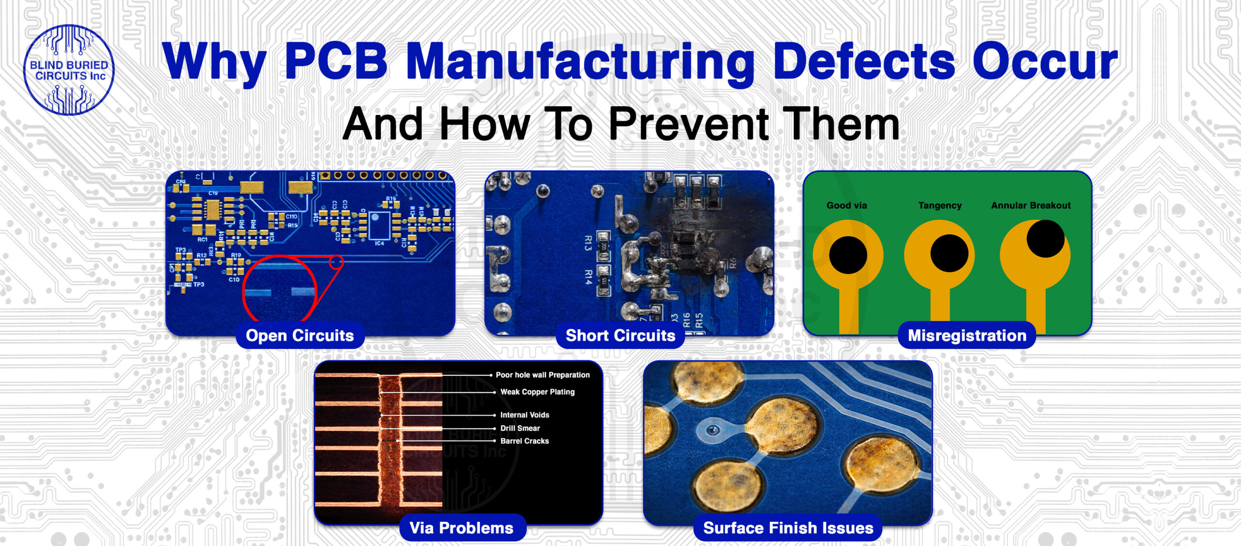
1) Open Circuits
Open circuits happen when the electrical path breaks somewhere on the board. This can be caused by a cracked copper trace, incomplete copper plating inside a via, over-etching during fabrication, or physical damage during handling.
Even a tiny break in the copper path can stop the signal completely. In real products, this may cause the board not to power on, a specific component to stop responding, or intermittent failures that are difficult to trace.
Common reasons include:
- broken traces
- incomplete via plating
- cracked copper after thermal stress
- drill damage
- over-etching
This is one of the most serious and most frequently reported PCB production issues because the board may look normal visually while the electrical path is already broken.
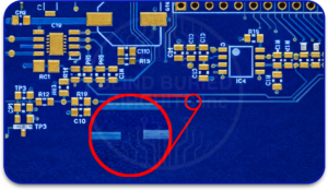
2) Short Circuits
Short circuits happen when two copper features that should stay separate accidentally connect. This unwanted copper bridge creates a direct electrical path between nets, often causing the board to fail immediately during test or power-up.
This defect often comes from:
- copper bridging after etching
- solder mask misalignment
- excess copper residue
- very tight spacing rules
- contamination during fabrication
Shorts are especially dangerous in high-density layouts because even a microscopic copper bridge can shut down the entire board or damage nearby parts during assembly.
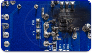
3) Misregistration
Misregistration happens when the layers inside a multilayer PCB do not line up properly during lamination.
In simple terms, the drilled holes, copper pads, and inner layers no longer match the original design position. This can create weak annular rings, off-center vias, broken interconnects, or signal integrity issues.
This defect is more common in:
- multilayer boards
- HDI designs
- blind and buried via structures
- fine-pitch layouts
The tighter the design, the more serious misregistration becomes. Even a small shift can make a via partially miss its target pad.
This is where strict fabrication control becomes essential, especially in advanced builds like those handled by Blind Buried Circuits, where internal layer precision matters even more than standard PCB work.
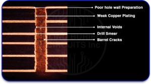
4) Via Problems
Via-related defects are among the most common production failures because vias connect signals between layers.
A via may fail due to:
- weak copper plating
- internal voids
- drill smear
- barrel cracks
- poor hole wall preparation
- thermal expansion stress
A via issue may not always fail immediately. Sometimes the board passes initial testing but later fails after heat cycles, vibration, or long-term field use.
This is why via defects are considered major reliability risks, especially in automotive, industrial, aerospace, and medical electronics.
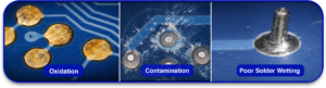
5) Surface Finish Issues
Surface finish problems affect how well components solder during assembly.
If the final finish is uneven, oxidized, contaminated, or too thin, solder joints may become weak, grainy, or inconsistent. This leads to poor wetting, cold joints, or rework during SMT assembly.
Common surface finish defects include:
- uneven ENIG thickness
- oxidation
- contamination
- poor solder wetting
- black pad risk
- rough copper finish
Even when the board is electrically correct, poor finish quality can create assembly failures later.
Solder Mask Defects PCB Teams Often Miss
One of the most overlooked problems is solder mask defects PCB teams discover only during assembly.
These include:
- mask misalignment
- bubbles
- incomplete coverage
- overexposed mask openings
- poor adhesion
- cracks after thermal cycling
These issues often come from:
- poor surface cleaning
- bad exposure settings
- curing temperature errors
- inaccurate artwork alignment
A small solder mask issue can lead to bridging, corrosion exposure, or weak insulation.
The most common prevention steps include:
- clean copper before coating
- verify exposure settings
- check curing profiles
- inspect openings under magnification
- run adhesion tests
This is especially important in HDI and multilayer builds where small pad clearances leave little room for error.
PCB Defects Causes In Design And Process
The biggest PCB defects causes are often shared between design and fabrication.
Design-Related Causes
- trace widths too small
- poor annular ring margins
- weak via structures
- tight spacing rules
- stack-up mismatch
- unrealistic tolerance assumptions
Process-Related Causes
- drill wander
- poor etch control
- copper thickness variation
- lamination pressure inconsistency
- contamination during plating
- poor bake cycles
This is where Blind Buried Circuits becomes especially relevant in the middle of the workflow, because blind and buried via structures require stronger DFM checks than standard boards.
Current PCB yield studies continue to show that most defect escapes are linked to rule margin issues and process drift rather than single isolated failures.
How To Prevent PCB Manufacturing Defects
The best way to reduce PCB manufacturing defects is to focus on prevention at every stage.
1) Start With DFM Reviews
Design for manufacturability checks should catch weak spacing, via, and stack-up risks.
2) Use Stable Materials
Choose laminates and copper weights that match the board’s thermal and electrical needs.
3) Tighten Process Controls
Key checkpoints should monitor:
- drill accuracy
- etch rates
- plating thickness
- lamination pressure
- solder mask cure
4) Increase Inspection
Use:
- AOI
- X-ray
- cross-section analysis
- impedance checks
- flying probe testing
5) Review Failure Trends
The best factories study repeat defects and fix the root cause, not just the failed board.
A simple prevention table:
| Defect Type | Best Prevention Step |
| Opens | Trace width and plating checks |
| Shorts | Spacing and AOI |
| Via Voids | Plating process control |
| Solder Mask Issues | Alignment and cure validation |
| Delamination | Material and lamination control |
Final Thoughts
Most PCB manufacturing defects are preventable when design teams and fabricators work together early.
The real solution is not just stronger final inspection. It is better DFM, stronger process discipline, tighter stack-up control, and early detection of drift. When these systems work together, defects become easier to predict and much less expensive to fix.
That is especially true for advanced multilayer and HDI builds, where hidden via structures increase risk. This is where Blind Buried Circuits becomes part of the larger reliability discussion, helping teams think about defect prevention from the first layout review.
CTA: Want Better PCB Yield And Fewer Defect Escapes? Start With Early DFM Checks And Process Controls Before Small Errors Reach Production.
FAQs
What Are The Most Common PCB Manufacturing Defects?
The most common issues include opens, shorts, via voids, misregistration, delamination, and solder mask defects.
What Causes PCB Defects Most Often?
The biggest causes are poor design margins, process drift, drilling errors, contamination, and weak inspection control.
How Do Solder Mask Defects PCB Problems Happen?
They usually happen because of poor cleaning, wrong exposure settings, bad alignment, or incomplete curing.
Can PCB Manufacturing Defects Be Prevented Early?
Yes. DFM checks, process monitoring, and strong inspection routines catch most issues early.
Why Are Via Defects So Serious?
Via defects can interrupt signal flow, weaken thermal paths, and reduce long-term reliability.
Why Do Multilayer Boards Need More Defect Control?
Because inner layers, blind vias, and buried vias create hidden failure points that are harder to inspect later.


