
Request our manufacturing capability
Capabilities
Controlled Impedance PCB Manufacturer
Our Capabilities
- Rigid PCB›
- PCB Assembly›
High-speed digital signals and RF circuits often require carefully controlled PCB trace impedance to maintain signal integrity and reliable transmission performance. Variations in trace width and spacing, copper thickness, dielectric thickness, material properties, and the relationship between traces and reference planes can affect the resulting impedance. As a controlled impedance PCB manufacturer, Blind Buried Circuits Inc addresses these requirements through design review, stackup development, and controlled fabrication processes. We manufacture rigid, flex, rigid-flex, multilayer, and HDI PCBs for applications requiring specified impedance characteristics. Whether your design includes a few impedance-controlled traces or a complex multilayer board with multiple impedance targets, our team reviews the design data and manufacturing specifications to produce PCBs in accordance with the specified electrical and dimensional requirements.
Controlled Impedance PCB Manufacturing Services Offered by Blind Buried Circuits Inc
Blind Buried Circuits Inc provides controlled impedance PCB fabrication services that address the key design, material, stackup, fabrication, and testing requirements for achieving specified impedance values. Here are the key PCB impedance control services we offer:
- Controlled Impedance PCB Fabrication: We manufacture boards according to the approved PCB data, material selection, layer stack-up, impedance values, and fabrication notes. The stack-up is reviewed as part of the manufacturing process because dielectric spacing and copper geometry directly affect impedance.
- Controlled Impedance PCB Design Support: Our engineering team can review PCB data and stack-up information for manufacturability. DFM and DFA review can help identify trace, via, material, or PCB assembly issues before fabrication begins.
- Impedance-Controlled Stack-Up Design: Our engineering team develops the PCB stack-up based on the required impedance values, copper thickness, dielectric thickness, material selection, and layer configuration. The stack-up is reviewed before fabrication to establish the required structure for impedance-controlled signal routing.
- Blind and Buried Via Fabrication: We manufacture PCBs with blind vias, buried vias, and microvias for high-density impedance-controlled designs. These structures support compact routing while maintaining the required layer connections and signal path configuration.
- Quick-Turn Controlled Impedance Prototypes: As a controlled impedance PCB manufacturer, we support prototype and validation builds for high-speed and RF applications. Prototype manufacturing allows engineering teams to verify PCB construction and impedance performance before moving into production.
- TDR Impedance Testing: We perform Time Domain Reflectometry (TDR) testing for impedance verification. Here, test coupons are included in the PCB panel to measure actual impedance values and compare them with the specified requirements.
- DFM and Stack-Up Review: Our engineering team reviews Gerber files, stack-up information, and fabrication requirements before production. This review helps identify trace geometry, material, via, and layer construction issues that may affect impedance or manufacturability.
- Turnkey PCB Assembly: We provide PCB fabrication, component procurement, assembly, and testing as part of a turnkey manufacturing service. We support SMT, through-hole, and mixed-technology assembly for controlled impedance PCB projects based on specific product requirements.

Controlled Impedance PCB Materials We Offer
Material selection is an important part of controlled impedance PCB construction. Laminates differ in dielectric constant (Dk), dissipation factor (Df), thermal characteristics, and fabrication requirements, all of which can influence electrical performance and manufacturability. We support a range of standard as well as specialty materials for high-speed, RF, high-temperature, and other demanding applications.
- FR-4 Materials: We offer FR-4 laminate options for controlled impedance PCBs, with material selection based on the required dielectric properties, stackup, trace geometry, and overall electrical performance.
- High-Frequency Materials: Our team works with Rogers and other specialty laminates for controlled impedance PCBs used in RF and high-frequency applications. These materials provide defined dielectric and low-loss characteristics and can be selected based on the required impedance, operating frequency, and signal-loss requirements.
- High-Tg Materials: We work with high-Tg laminates for controlled impedance PCBs used in applications with elevated processing or operating temperatures. These materials can be selected based on the required impedance, thermal requirements, layer stack-up, and operating conditions.
- PTFE Flex Materials: We support PTFE-based flex materials for applicable high-frequency and impedance-controlled flexible circuits. Material selection can be based on the required dielectric characteristics, impedance, operating frequency, flexibility, and signal-loss requirements.
- Polyimide Flex Materials: We use polyimide materials for impedance-controlled flex and rigid-flex PCBs where flexibility and electrical performance need to be considered together. These materials can be selected based on the required impedance, dielectric thickness, circuit construction, and mechanical requirements.
Why Choose Controlled Impedance PCBs?
Here are some benefits of choosing controlled impedance PCBs.
- Maintains Signal Integrity at High Speeds: As signal speeds increase, PCB traces behave like transmission lines. Controlled impedance PCBs are engineered to maintain the required impedance throughout the signal path, helping reduce reflections, signal distortion, and timing issues that can affect circuit performance.
- Supports Predictable Electrical Performance: A controlled impedance PCB provides a defined transmission-line structure to help maintain predictable electrical performance. Depending on the interface requirements, the target impedance may be specified as either single-ended or differential impedance.
- Greater Design Predictability: By controlling factors that influence impedance, such as trace geometry, material properties, dielectric thickness, copper thickness, and layer stackup, controlled impedance PCBs help maintain specified impedance values within defined tolerances. This provides greater predictability as the design progresses from validation and prototyping to production.
- Optimized PCB Stack-Up: Controlled impedance PCBs use a defined stackup in which trace geometry, dielectric thickness, material properties, and reference-plane relationships are specified to achieve the target impedance within the required tolerance. This helps maintain predictable signal behavior across impedance-controlled traces.
Controlled Impedance PCB Applications
Controlled impedance PCBs are used in electronic products where signal transmission must remain within defined electrical limits. Here are the industries we support with our controlled impedance PCB fabrication services.
- Telecommunications: Networking equipment, communication hardware, routers, switches, and related systems can require controlled impedance routing for high-speed data transmission.
- Aerospace and Avionics: Controlled impedance PCBs are used in avionics, communication, sensor, and control systems where high-speed signal transmission and predictable electrical performance are important.
- Automotive Electronics: Advanced vehicle electronics use high-speed communication, sensors, control systems, and other circuits that can require impedance-controlled signal paths.
- Medical Electronics: Imaging equipment, diagnostic systems, monitoring equipment, and other medical electronics can use high-density multilayer PCBs with controlled signal routing.
- Industrial Automation: Industrial controls, measurement equipment, robotics, sensors, and factory automation systems can benefit from controlled impedance PCB design.
- Consumer Electronics: Products containing processors, displays, wireless communication, and high-speed interfaces may require controlled impedance PCB construction.
Why Choose Blind Buried Circuits Inc for Controlled Impedance PCB Manufacturing?
Blind Buried Circuits Inc provides controlled impedance PCB manufacturing for rigid, flex, rigid-flex, multilayer, HDI, and prototype PCB boards. Our manufacturing capabilities support impedance requirements across different PCB constructions, materials, and layer configurations based on project specifications.
- Engineering Support: Our engineering team reviews design files, impedance requirements, stackup configurations, material selections, and key manufacturability considerations to help ensure the PCB design is suitable for controlled impedance fabrication.
- Turnkey Manufacturing: We coordinate PCB fabrication, component procurement, assembly, and related manufacturing services through a single source, helping streamline the overall production process.
- Quality Certifications: Blind Buried Circuits has ISO 9001:2015, ISO 13485:2016, ISO 14001:2015, IPC-A-600, IPC-A-610, RoHS, and UL certifications.
- Prototype and Production Support: We support engineering prototypes as well as larger production requirements.
- Responsive Quotation Process: We can provide pricing within 24 hours for applicable turnkey projects, while actual production lead time depends on the circuit and manufacturing requirements.
Frequently Asked Questions
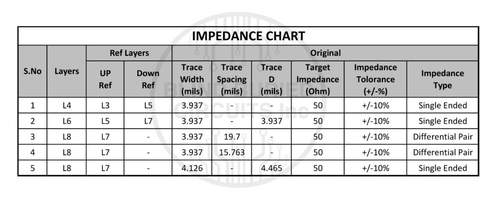
Yes. Different signal layers can have different impedance requirements because their dielectric spacing, reference planes, copper thickness, and trace geometry may differ. The fabrication documentation should clearly identify the controlled impedance nets and their target values.
Yes. Differential pairs have their own impedance requirement based on trace width, spacing, dielectric construction, and reference-plane configuration. The PCB stack-up should account for both differential and single-ended signal requirements where both are present.
Yes. A via creates a transition between PCB layers and can introduce discontinuity into a high-speed signal path. Via diameter, pad size, anti-pad geometry, stub length, and surrounding copper can all affect the transition. HDI microvias can be useful in designs where shorter signal transitions are required.
: In many cases, an existing design can be modified, but the feasibility depends on the current layer count, routing, materials, available board thickness, and impedance targets. Changes to trace width or dielectric spacing may require layout revisions, so an engineering review is critical before fabrication.
Ready To Get Started?
To learn more about our PCB Design Guidelines, don’t hesitate to contact our sales team at sales@blindburiedcircuits.com.