

Objective
To compare HASL and ENIG PCB finishes, their benefits, limitations, and applications, helping engineers choose the right surface finish.
Key Takeaways
- HASL: Cost-effective and suitable for conventional PCB assemblies.
- ENIG: Flat, uniform finish ideal for BGA, QFN, and fine-pitch SMT.
- Cost: HASL is generally cheaper; ENIG offers better pad flatness.
- Selection: Depends on PCB design, component layout, and assembly requirements.
Table Of Contents
-
-
- Introduction
- What Is a PCB Surface Finish and Why Does It Matter?
- What Is HASL PCB Finish?
- What Is ENIG PCB Finish?
- HASL vs. ENIG PCB: Key Differences
- How Does ENIG Plating Work? The ENIG PCB Plating Process Step by Step?
- ENIG PCB Surface Finish Thickness
- HASL vs. ENIG vs. Other PCB Surface Finishes
- Which PCB Surface Finish Is Better?
- Advantages and Disadvantages of HASL vs. ENIG PCB
- Applications of HASL PCB
- Applications of ENIG PCB
- How to Choose the Right PCB Surface Finish for Blind and Buried Via PCBs?
- Why Choose Blind Buried Circuits for Your PCB Projects?
- Frequently Asked Questions
-
Introduction
Choosing the right PCB surface finish can affect solderability, assembly quality, manufacturing costs, and long-term reliability. Two commonly used options are Hot Air Solder Leveling (HASL) and Electroless Nickel Immersion Gold (ENIG).
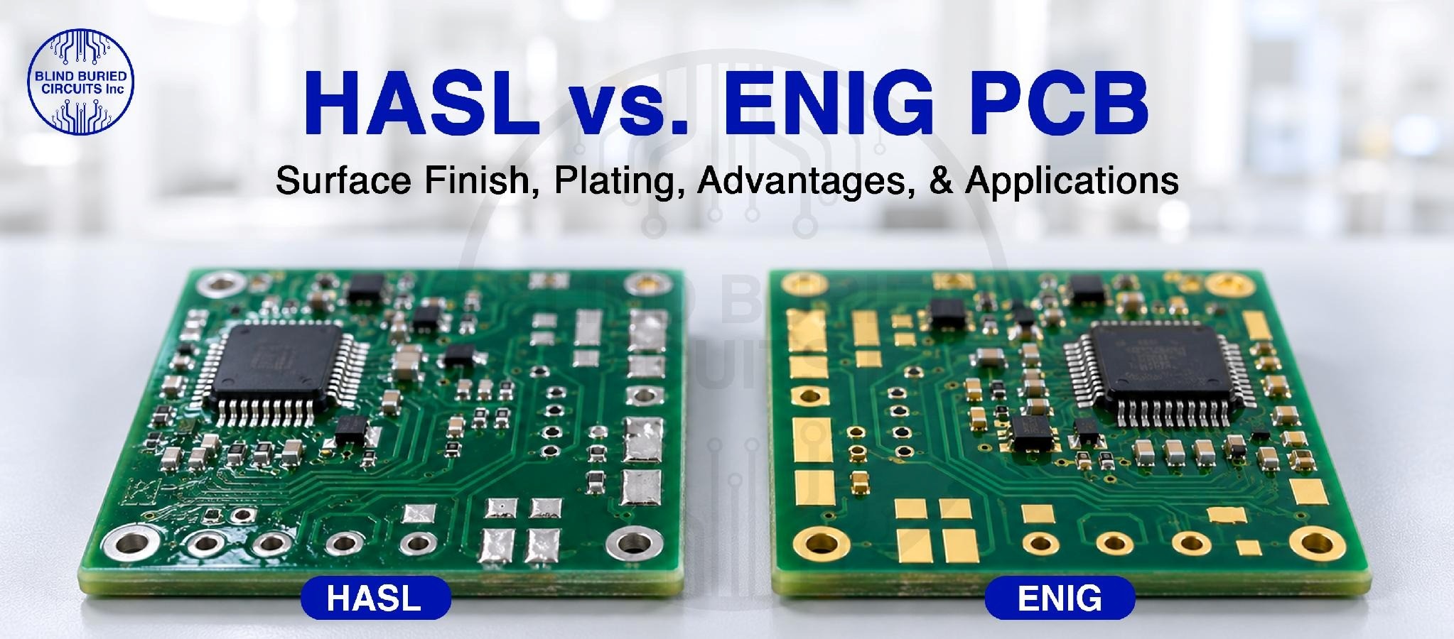
The key difference between HASL and ENIG PCB finishes is surface flatness and cost. HASL offers an economical solder coating for conventional PCB designs, while ENIG provides a flatter surface suited to fine-pitch components, BGA packages, and high-density assemblies.
So, which surface finish is right for your PCB project? Let’s compare their plating processes, advantages, limitations, and applications.
What Is a PCB Surface Finish and Why Does It Matter?
A PCB surface finish is a protective coating applied to exposed copper pads and other designated conductive areas. It prevents copper oxidation and helps maintain solderability during assembly.
The right finish can influence solder-paste printing, component placement, solder-joint quality, and manufacturing costs.
For example, conventional PCB layouts may work well with HASL, while designs with closely spaced components often benefit from the flatter surface of ENIG.
What Is HASL PCB Finish?
Hot Air Solder Leveling (HASL) is a PCB surface finishing process that coats exposed copper with a solder alloy.
During manufacturing, the board is treated with flux and exposed to molten solder. Hot air knives then remove excess solder, leaving a protective coating on the copper pads.
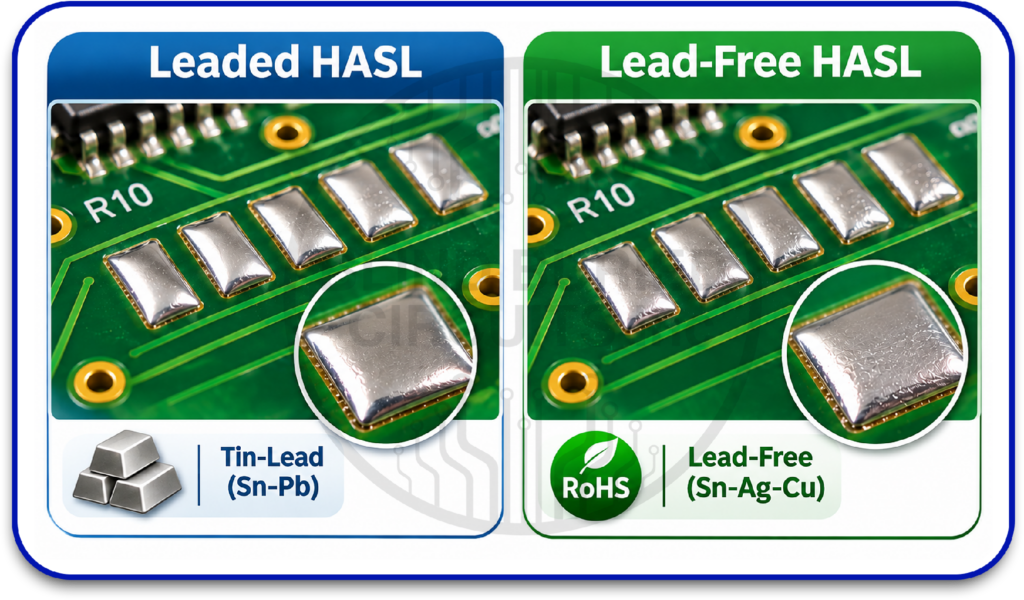
There are two main types of HASL PCB finishes:
- Leaded HASL: Uses a tin-lead solder alloy and is suitable for applications where lead-containing finishes are permitted.
- Lead-Free HASL: Uses a lead-free solder alloy and is commonly selected for electronics subject to RoHS requirements.
HASL offers good solderability at a relatively low cost. However, its solder coating may vary in thickness, making it less suitable for certain fine-pitch SMT assemblies.
What Is ENIG PCB Finish?
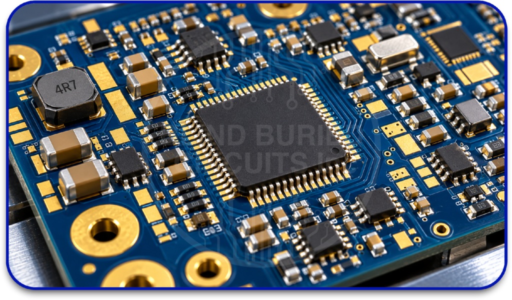
Electroless Nickel Immersion Gold (ENIG) is a chemical surface finish that deposits a nickel layer over exposed copper, followed by a thin gold coating.
The nickel acts as a barrier between the copper and solder, while the gold protects the nickel from oxidation before assembly.
An ENIG PCB surface finish provides a flat, uniform surface, making it particularly useful for:
- Ball Grid Array (BGA) packages
- Quad Flat No-Lead (QFN) components
- Fine-pitch SMT assemblies
- High-density interconnect (HDI) PCBs
- Complex multilayer circuit boards
Although ENIG PCB plating generally costs more than HASL, its surface uniformity makes it a practical choice for demanding component layouts.
HASL vs. ENIG PCB: Key Differences
| Comparison Factor | HASL PCB | ENIG PCB |
|---|---|---|
| Composition | Tin-based solder alloy | Electroless nickel and immersion gold |
| Surface Flatness | Uneven solder coating | Flat, uniform coating |
| Manufacturing Cost | Generally lower | Generally higher |
| Solderability | Good when properly processed | Good when properly plated |
| Fine-Pitch Compatibility | Less suitable for some fine-pitch components | Well suited for BGA, QFN, and fine-pitch SMT |
| Manufacturing Process | Molten solder and hot-air leveling | Chemical nickel and gold deposition |
| Thermal Exposure | High temperatures during finishing | No molten-solder leveling step |
How Does ENIG Plating Work? The ENIG PCB Plating Process Step by Step?
The ENIG PCB plating process involves four main stages.
| Step | Process | Purpose |
|---|---|---|
| 1 | Surface preparation | Removes contaminants and prepares exposed copper |
| 2 | Electroless nickel plating | Deposits a nickel-phosphorus barrier layer without external electrical current |
| 3 | Immersion gold plating | Adds a thin gold coating to protect the nickel |
| 4 | Inspection | Checks coating thickness, coverage, and finish quality |
During soldering, the thin gold layer dissolves into the molten solder. Tin then reacts with the underlying nickel to form intermetallic compounds that contribute to the solder joint.
Consistent plating chemistry and process control are essential for maintaining ENIG finish quality.
ENIG PCB Surface Finish Thickness
ENIG PCB surface finish consists of two plating layers:
- Electroless Nickel (3–6 µm): Acts as a barrier between copper and solder, supporting solderability and reliable solder joints.
- Immersion Gold (0.05–0.10 µm): Protects the nickel layer from oxidation and helps maintain solderability before assembly.
These are typical industry thickness ranges. Actual ENIG plating requirements should follow the applicable IPC-4552 specification and project-specific manufacturing requirements.
HASL vs. ENIG vs. Other PCB Surface Finishes
Besides HASL and ENIG, PCB manufacturers use other finishes, including Organic Solderability Preservative (OSP), immersion silver, and Electroless Nickel Electroless Palladium Immersion Gold (ENEPIG).
Each offers different benefits depending on solderability, cost, surface flatness, and assembly requirements.
| PCB Surface Finish | Key Characteristics | Typical Applications |
|---|---|---|
| HASL | Economical, good solderability, but uneven pad surfaces | Conventional PCBs, through-hole assemblies |
| ENIG | Flat nickel-gold coating with good oxidation protection | BGA, QFN, fine-pitch SMT, HDI PCBs |
| OSP | Low-cost, flat organic coating; requires careful handling | High-volume, cost-sensitive PCB assemblies |
| Immersion Silver | Flat, solderable coating; requires tarnish control | Fine-pitch and nickel-free designs |
| ENEPIG | Nickel-palladium-gold finish compatible with certain wire-bonding processes | Advanced electronics and specialized assemblies |
For conventional designs, HASL PCB is often an economical option. ENIG PCB finish is commonly preferred when fine-pitch assembly requires consistent pad flatness.
Which PCB Surface Finish Is Better?
- Choose HASL when manufacturing cost is a priority and your design uses conventional component spacing or through-hole assembly.
- Consider ENIG when your PCB includes fine-pitch components, BGA packages, or dense SMT layouts requiring a more uniform pad surface.
Neither finish is universally better. The right choice depends on your design and assembly requirements.
Advantages and Disadvantages of HASL vs. ENIG PCB
Advantages of HASL PCB
- Lower manufacturing cost, making it suitable for budget-conscious projects.
- Good solderability for conventional PCB assemblies.
- Suitable for through-hole components and standard PCB designs.
- Widely used and established manufacturing process.
Disadvantages of HASL PCB
- Uneven solder coating can affect pad flatness.
- Less suitable for certain fine-pitch SMT components.
- High processing temperatures may stress thermally sensitive boards.
- Leaded HASL may not meet applicable RoHS requirements.
Advantages of ENIG PCB
- Flat, uniform surface suitable for BGA, QFN, and fine-pitch SMT assembly.
- Good solderability and oxidation protection.
- Good storage stability under suitable conditions.
- Supports consistent solder-paste printing and component placement.
Disadvantages of ENIG PCB
- Higher manufacturing cost compared with HASL.
- Requires careful control of the ENIG plating process.
- Improper plating can cause nickel corrosion and black pad defects.
- Not a direct replacement for hard gold in high-wear connector applications.
Applications of HASL PCB
HASL is commonly used in PCB designs where cost-effectiveness and reliable solderability are important, and highly uniform pad surfaces are not essential.
Typical applications include:
- Through-hole assemblies: Boards containing conventional through-hole components.
- Consumer electronics: General-purpose devices with standard component layouts.
- Power supply boards: Power management and conversion circuits with compatible pad geometries.
- Industrial control systems: Control and interface boards with conventional component spacing.
- Cost-sensitive PCB projects: Applications where an economical finish meets assembly requirements.
However, HASL may not be suitable for some fine-pitch components because of variations in solder coating thickness.
Applications of ENIG PCB
ENIG PCB plating is widely used in designs that require flat solder pads and consistent surface quality.
Common applications include:
- Fine-pitch SMT assemblies: Closely spaced surface-mount components.
- BGA and QFN packages: Components that benefit from uniform solder-pad surfaces.
- HDI and multilayer PCBs: Dense circuit layouts with demanding assembly requirements.
- Telecommunications equipment: Compact circuit boards with high component density.
- Medical and aerospace electronics: Designs with specified surface quality and assembly requirements.
- Advanced computing hardware: High-density boards using fine-pitch components.
ENIG is particularly useful when pad flatness is important for solder-paste printing and component placement.
How to Choose the Right PCB Surface Finish for Blind and Buried Via PCBs?
Not sure whether HASL or ENIG is right for your blind and buried via PCB?
Blind and buried vias help designers create compact, high-density circuit layouts. However, the via structure itself does not determine which surface finish you need.
Here are a few questions to consider before making your decision:
- Working with fine-pitch components? ENIG provides a flatter surface for BGAs, QFNs, and closely spaced SMT components. HASL may be sufficient for standard component layouts.
- What does your assembly process require? Consider solder-paste printing, component placement, and soldering methods before selecting a finish.
- Does your PCB have exposed contacts? Connector fingers and contact areas may require specialized finishes. Hard gold is often more suitable than ENIG for repeated-contact wear.
- Is manufacturing cost a priority? HASL is generally more affordable, while ENIG requires additional plating processes.
- How important is reliability? Evaluate solder-joint performance, storage conditions, and plating quality. Proper process control helps minimize ENIG defects such as black pad.
- Are there regulatory requirements? If your product is subject to RoHS restrictions, confirm the surface finish and other materials meet the applicable requirements.
The best approach is to discuss your PCB stack-up, component layout, via design, and assembly requirements with your fabricator before finalizing the surface finish.
Why Choose Blind Buried Circuits for Your PCB Projects?
At Blind Buried Circuits Inc, we provide PCB manufacturing and assembly solutions for projects ranging from prototypes to production.
Our capabilities include multilayer PCBs, HDI designs, and blind and buried via technology, with surface finish options such as HASL and ENIG.
We support Design for Manufacturing (DFM), PCB fabrication, component sourcing, and assembly to help customers balance quality, cost, and manufacturing requirements.
Whether you’re developing a conventional PCB or a complex fine-pitch assembly, our team can help you evaluate your design and move your project toward production.
Ready to get started? Request a PCB Quote and share your Gerber files, BOM, quantities, and assembly requirements with our team.