

Objective
Explain what a castellated PCB is, how it is made and designed, where it is used, and how to choose a manufacturer, so OEMs can mount compact modules directly onto a carrier board.
Key Takeaways
- A castellated PCB has plated half-holes along its edges that act as solderable contacts.
- It is soldered directly to a carrier board, with no pin header or connector needed.
- The format lowers assembly height and component count for compact modules.
- Hole size, pitch, edge clearance, and pad design should be confirmed with the fabricator early.
- Choose a manufacturer with proven castellated hole experience, DFM review, and quality inspection.
Table Of Contents
- Introduction
- What Is a Castellated PCB?
- What Are Castellated Holes and Castellated Pads?
- How Are Castellated Holes Manufactured?
- Castellated Board Edge Connectors and Castellated PCB Socket Options
- Castellated Edges vs. Other Connection Methods
- Castellated PCB Types and Variations
- Castellated PCB Design Guidelines
- Advantages of Castellated Circuit Boards
- Applications of Castellated PCBs
- How to Choose a Castellated PCB Manufacturer?
- Why Choose Blind Buried Circuits Inc for Your Projects?
- Frequently Asked Questions
Introduction
A compact wireless module may need to be mounted directly onto a carrier board where enclosure space is limited. A pin header can increase assembly height, while a board-to-board connector adds components, cost, and another mechanical interface.
Castellated PCBs offer an alternative approach for connecting compact boards in space-constrained applications. This guide explains what a castellated PCB is, how castellated holes and edges work, how these boards are manufactured, how to design them, where they are used, and what OEMs should consider when selecting a manufacturer.
What Is a Castellated PCB?
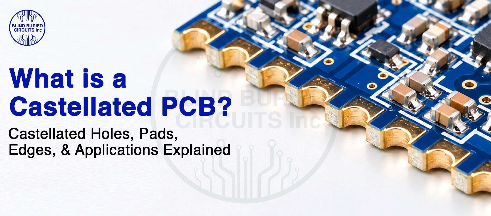
A castellated PCB is a circuit board with plated half-holes formed along one or more edges. From the side, the openings resemble the notches of a castle wall, which gives the technology its name.
The construction is also described using terms such as castellated edges, castellated holes, half-cut holes, and edge-plated holes. Terminology can vary between PCB designers, manufacturers, and module suppliers.
During fabrication, plated holes are positioned close to the planned board outline. The board is then routed through or along the plated holes, leaving plated semicircular openings along the edge. The exposed copper and plating provide a solderable termination.
This allows one PCB to be soldered directly onto a carrier board using the castellated edge as the soldering interface. Depending on the design, this can eliminate the need for a separate pin header or mating connector between the two boards.
For compact wireless, control, sensing, and communications modules, this approach can help reduce assembly height and simplify board-to-board integration.
What Is a Castellated PCB?
Castellated holes are plated through-holes located along the PCB edge and partially exposed when the board outline is formed. After the board outline is routed, only part of each plated hole remains.
Castellated pads refer to the exposed, solderable portions of the plated holes along the board edge. In practice, the two terms are sometimes used interchangeably, although a hole describes the plated opening while a pad describes the solderable contact area.
Hole diameter, pitch, copper thickness, annular ring, and edge clearance all affect the finished structure. These dimensions must be compatible with both the module and the carrier-board footprint.
The carrier PCB normally has matching surface-mount pads. During soldering, molten solder wets the exposed plated surfaces and forms the electrical and mechanical connection.
On multilayer PCB boards, the hole structure and internal copper geometry should also be reviewed carefully so that edge routing does not unintentionally expose or damage internal conductors.
What Are Castellated Holes and Castellated Pads?
The connection process involves aligning the module with the carrier PCB and forming solder joints between their corresponding contacts.
- Board Alignment: The module is positioned so that its castellated holes align with corresponding surface-mount pads on the carrier PCB.
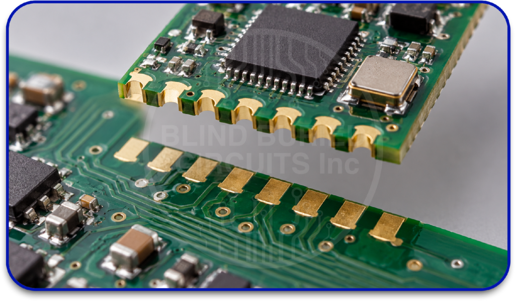
Solder Contact: During reflow, solder on the carrier-board pads melts and wets the exposed plated surfaces of the castellated holes.
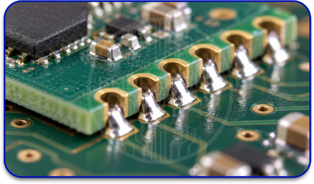
Electrical Connection: Once the solder solidifies, it forms a conductive joint between each castellated contact and its corresponding carrier-board pad, allowing signals and power to pass between the two PCBs.
Mechanical Attachment: The soldered joints also secure the module to the carrier board, with the strength of the connection depending on factors such as pad geometry, solder joint formation, and board design.
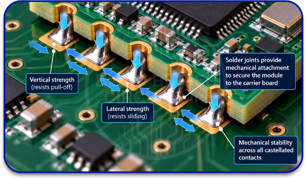
Completed PCB-to-PCB Connection: The resulting solder joints provide electrical connectivity and physical attachment without requiring a separate pin header or mating connector.
How Are Castellated Holes Manufactured?
Castellated PCB fabrication involves multiple stages, including:
- Drilling: Holes are drilled close to the planned board outline. Hole diameter, position, and spacing must remain within the manufacturer’s process limits.
- Hole Plating: The drilled holes receive conductive copper plating. This creates the electrical path through the hole and provides the plated surface that remains exposed after edge routing.
- Edge Routing: The PCB outline is routed through the plated holes, removing part of each hole and creating the characteristic plated semicircular openings.
- Routing Accuracy: Precise routing helps maintain consistent castellation dimensions. Poor control can produce uneven edges, burrs, or damage to the plated surfaces.
- Edge Finishing: Deburring and cleaning help remove unwanted material and maintain a suitable edge condition for assembly and inspection.
- Surface Finish: Common options include ENIG, HASL, immersion silver, and immersion tin. The appropriate finish depends on the PCB design, assembly process, and manufacturer capabilities.
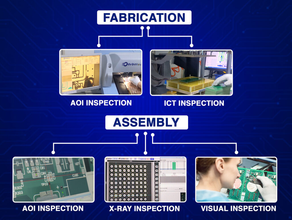
- Inspection: Inspection should verify plating continuity, hole and edge position, exposed plated-surface condition, burr control, and overall castellation geometry.
- Fabrication Review: Castellated hole requirements should be reviewed with the PCB manufacturer before production. Early review can identify drilling, plating, routing, and dimensional limitations before the design reaches fabrication.
Castellated Board Edge Connectors and Castellated PCB Socket Options
A castellated board is normally soldered directly to its carrier PCB. Unlike an edge-card connection, it is not generally intended to plug into a conventional connector.
A castellated PCB socket or socket-style fixture can still be useful during development and testing when a module needs to be removed and reinstalled without soldering and desoldering each time.
Uses:
- Development and Prototyping: Temporary module mounting during firmware and hardware development.
- Programming: Access to a module for programming without permanently soldering it to each test fixture.
- Production Testing: Repeatable temporary connections for programming or functional testing.
- Engineering Evaluation: Convenient removal and replacement during design validation.
- Final OEM Assembly: Direct soldering remains a common approach where a permanent connection is required.
Castellated Edges vs. Other Connection Methods
A castellated PCB is one option among several board-to-board connection methods. The appropriate approach depends on the required profile, connection type, serviceability, and assembly requirements.
| Method | Height | Cost | Serviceability | Typical use |
|---|---|---|---|---|
| Castellated edges | Low | Low to moderate | Low | Permanently mounted modules |
| Pin headers | Moderate to high | Low to moderate | High | Prototypes and removable modules |
| Board-to-board connectors | Low to moderate | Moderate to high | High | Removable or serviceable modules |
| LGA/BGA modules | Very low | Moderate to high | Low | Dense production assemblies |
| Edge-card connectors | Moderate | Moderate to high | High | Removable boards |
The choice depends on whether the product requires a permanent or removable connection, a low-profile design, easier service access, or a high-density interconnection.’
Castellated PCB Types and Variations
Castellated PCBs can be produced in several configurations, depending on the module footprint, carrier-board layout, and connection requirements.
- Single-Sided vs. Double-Sided: Castellated contacts can be formed with plated surfaces exposed on one or both sides of the board edge, depending on the board construction and assembly design. The configuration should provide the required contact area while maintaining adequate clearance for soldering and assembly.
- Full-Edge vs. Partial-Edge: Castellations can run along an entire board edge or occupy selected sections. Partial placement is useful when parts of the edge require mechanical clearance, mounting features, or other board-level connections.
- Rigid, Multilayer, and HDI Boards: Castellated features can be incorporated into standard rigid PCBs as well as multilayer and HDI constructions. On HDI boards, they can work alongside microvias and other dense interconnect structures to support compact module layouts.
- Fine-Pitch vs. Standard-Pitch: Fine-pitch castellations suit small, high-density modules, while larger pitches can provide more room for drilling, plating, routing, solder mask, and assembly. The practical limit depends on the PCB manufacturer’s process capabilities.
For dense OEM assemblies, the castellation configuration should be established with the fabricator during the design stage. A pitch or edge layout that appears suitable in CAD still needs to meet the manufacturer’s requirements for fabrication, soldering, and inspection.
Castellated PCB Design Guidelines
Castellation performance depends on the PCB footprint and edge-feature geometry. Small dimensional changes can affect solder coverage, mechanical strength, and manufacturability. Key design points include:
| Design Factor | What to Check |
|---|---|
| Hole diameter | Confirm the minimum practical drill size with the fabricator. |
| Size and Pitch | Match the castellated hole geometry to the assembly process and carrier footprint. |
| Edge clearance | Leave sufficient material around the plated hole and board outline. Keep traces, vias, and other copper features away from the castellation zone unless they are intentionally part of the connection. |
| Pad geometry | Ensure the carrier-board pads provide sufficient area for soldering and alignment with the castellated contacts. |
| Annular ring | Confirm that the plated hole retains sufficient copper around the drilled hole and after the board edge is formed. |
| Traces and vias | Keep routing and vias clear of the castellation zone unless they are intentionally connected to the castellated feature. |
| Solder mask | Make sure the mask opening exposes the required plated area without unnecessarily reducing the solderable surface. |
| Silkscreen | Keep reference markings away from solderable areas. |
| Panelization | Position routing tabs and breakaway features away from castellations so they do not damage the plated edge during depaneling. |
Advantages of Castellated Circuit Boards
A castellated circuit board offers a practical connection method for compact modules that need to mount directly onto a carrier PCB. The key advantages include:
- No Separate Connector or Header: The PCB itself provides the solderable electrical contacts, eliminating the need for a separate header or connector in compatible designs.
- Low-Profile Assembly: Direct PCB-to-PCB mounting can help reduce overall assembly height compared with some connector-based configurations.
- Lower Component Count: Eliminating an intermediate connector can reduce the number of interconnection components in the assembly.
- Direct Electrical Connection: Signals and power can pass directly from the module into the carrier PCB through the soldered castellated connections.
- Distributed Mechanical Attachment: Multiple soldered castellations distribute the attachment points along the module edge, with overall joint strength depending on the board and solder-joint design.
- Good for Compact Modules: The format is well suited to wireless, sensing, processing, and control modules where direct PCB-to-PCB mounting is appropriate.
- Suitable for Prototypes and Production: The same basic connection concept can be used for prototyping and volume production when the design and assembly process support it.
Applications of Castellated PCBs
Castellated PCBs are common in module-based electronics where space is limited and the module needs a direct connection to the main board. Typical applications include:
- IoT and wireless products: Wi-Fi, Bluetooth, cellular, and other communication modules can mount directly to a host PCB.
- Wearables and consumer electronics: The low-profile connection can help conserve enclosure space in compact electronic products.
- Medical equipment: Sensor, communications, and processing modules can be integrated into compact electronic assemblies where the connection method meets the applicable design and reliability requirements.
- Instrumentation: Castellated modules can provide a convenient way to integrate sensing and control functions.
- Automotive electronics: Compact controller and communications modules can benefit from a soldered board-to-board connection when the design meets the required automotive environmental and reliability conditions.
- Industrial controls: Embedded processing, sensing, and communications modules can be mounted directly onto control boards.
- Aerospace and communications equipment: Space-efficient module integration can be useful in applications where board area and mechanical packaging are tightly controlled, subject to the required reliability and qualification criteria.
How to Choose a Castellated PCB Manufacturer?
OEMs should assess more than general PCB fabrication capability. Look specifically for experience with castellated hole PCB production and the process controls these features require.
- Check Castellated PCB Fabrication Experience: Choose a manufacturer experienced in castellated holes, edge routing, plating, edge finishing, and inspection. Ask about previous applications with similar board dimensions, hole sizes, and pitch requirements.
- Verify Drilling, Plating, and Routing Capability: Confirm the manufacturer’s minimum drill diameter, hole pitch, plating control, and routing accuracy for your castellated PCB design. These capabilities directly affect the finished hole profile and edge geometry.
- Review Materials and Surface Finishes: Confirm that the manufacturer can provide the required laminate, copper thickness, and surface finish, based on your electrical, mechanical, and assembly requirements.
- Assess Multilayer and HDI Capability: For dense designs, verify that the manufacturer can incorporate castellations into multilayer and HDI PCBs while maintaining the required clearances and internal-layer connections.
- Request DFM and Engineering Review: Use a pre-production review to identify potential issues with hole placement, edge clearance, pad geometry, solder mask, routing, and panelization before fabrication.
- Evaluate Quality and Inspection: Review the manufacturer’s quality systems, dimensional controls, plating inspection, and methods for verifying castellated features. This helps establish whether the supplier can maintain consistent results across production runs.
- Consider Production Capacity and Support: Evaluate whether the manufacturer can support prototype quantities and production volumes, along with reasonable lead times and responsive engineering support when design or manufacturing issues arise.
Why Choose Blind Buried Circuits Inc for Your Projects?
Blind Buried Circuits Inc provides PCB fabrication support for designs with castellated edges and other advanced interconnect requirements.
- Advanced PCB Construction: Support for multilayer and HDI boards, including blind and buried via structures for dense module designs.
- Castellated PCB Requirements: Review of castellated hole geometry, board construction, materials, and edge-routing requirements during project evaluation.
- Engineering Review: Early review of PCB design files to identify potential fabrication concerns before production.
- Project Documentation: Review of PCB files, stack-up requirements, castellated edge details, surface finish, and application requirements to establish the required construction.
- OEM Project Support: Project-specific fabrication support based on technical requirements, production volume, and application needs.
- Quotation Support: Project-specific quotations for new castellated PCB designs and existing designs requiring fabrication support.
Engage Blind Buried Circuits Inc early to review your design, confirm fabrication requirements, and request a project-specific quotation for your castellated PCB project.