

Objective
This guide explains whether PCB solder resist and solder mask are the same, and helps you choose the right circuit board solder mask for rigid, BGA, flex, and blind and buried via boards.
Key Takeaways
-
- PCB solder resist and PCB solder mask are the same coating. Only the regional name differs.
- It prevents solder bridging, insulates copper, and protects the board.
- PCB solder mask material is mostly epoxy-based. Flex boards use polyimide coverlay or flexible mask.
- LPI is the most common type, and green is the most common color.
- Blind vias may be exposed, tented, plugged, or filled, while buried vias need no mask opening.
- A DFM review and fabricator check prevent most defects.
Table Of Contents
- Introduction
- What Is PCB Solder Resist?
- What Is a PCB Solder Mask?
- How to Choose the Right Solder Resist or Solder Mask for Your PCB
- Solder Resist vs. Solder Mask: Is There Any Difference?
- How Is Solder Resist or Solder Mask Applied to a Circuit Board?
- Solder Resist Materials Used in PCB Fabrication
- Types of PCB Solder Resist and Solder Mask
- What Are the Popular PCB Solder Mask Colors?
- Applications of PCB Solder Mask: Standard, BGA, Flex, and Blind Buried Via PCBs
- Common Solder Resist and Solder Mask Defects and How to Prevent Them
- How to Choose the Right Solder Resist or Solder Mask for Your PCB
- Why Choose Blind Buried Circuits for Your PCB?
- Frequently Asked Questions
Introduction
In printed circuit board (PCB) manufacturing, a thin protective coating covers the copper traces on the outer layers of the board. Depending on the region and the supplier, that coating is called PCB solder resist or PCB solder mask. It helps prevent solder bridging during assembly, insulates copper conductors, and protects the board in service. Choosing the right PCB solder mask material and process matters for everything from standard rigid boards and BGA layouts to flexible circuits and multilayer boards with blind and buried vias. This guide explains whether solder resist and solder mask are the same, and covers materials, types, colors, applications, common defects, and how to choose the right option for blind buried circuit boards.
What Is PCB Solder Resist?
PCB solder resist is a permanent polymer coating applied to selected areas of a printed circuit board. It covers copper traces while leaving solder pads, test points, and other designated contact areas exposed. “Solder resist” is the term most commonly used in the UK, Europe, and many Asian markets.
The coating serves several purposes:
- Prevents solder bridging: It keeps molten solder from flowing between closely spaced pads and conductors during assembly.
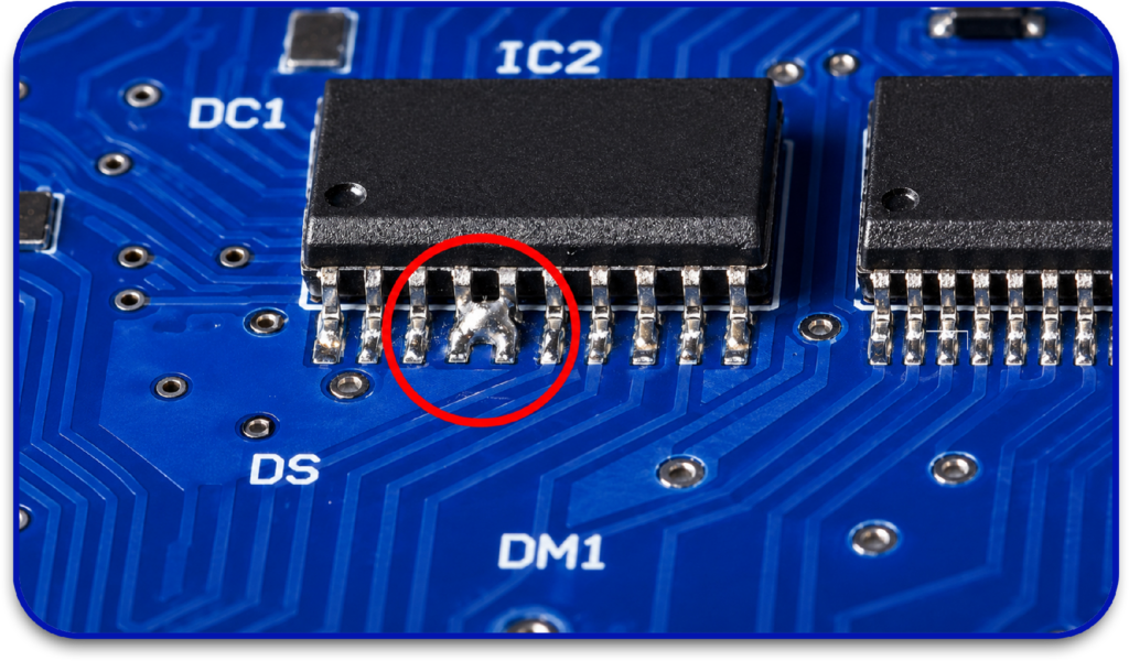
Provides electrical insulation: It insulates adjacent copper features from each other and from accidental contact.
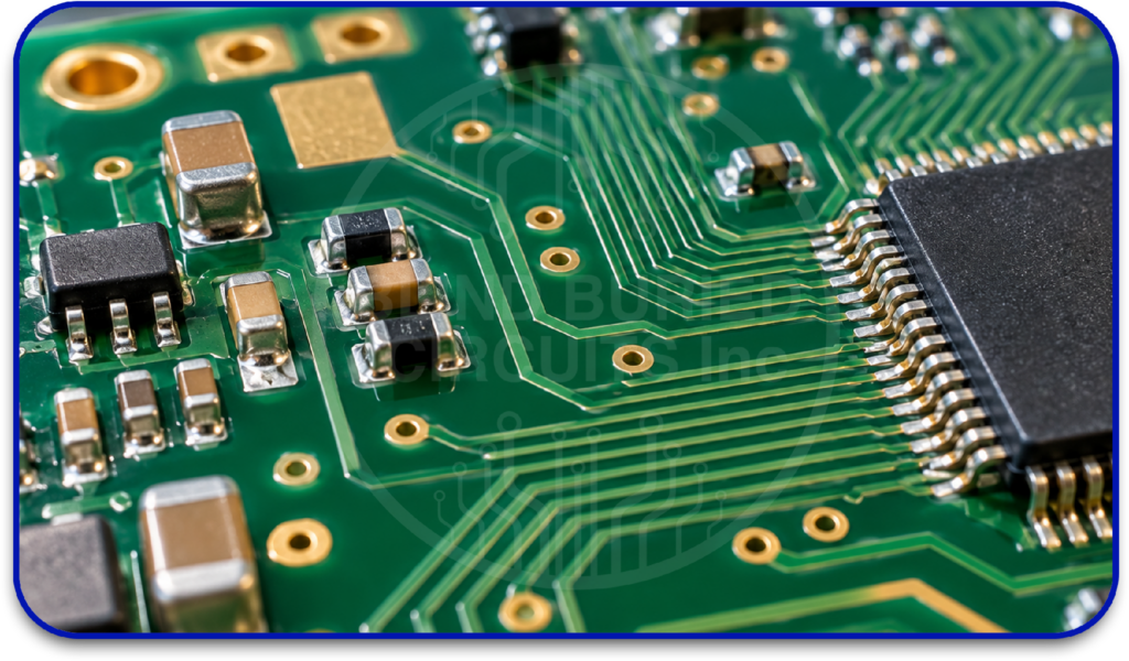
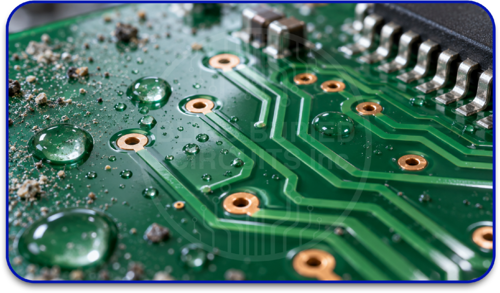
Protects the copper: It helps shield traces from oxidation, moisture, dust, and other contamination.
What Is a PCB Solder Mask?
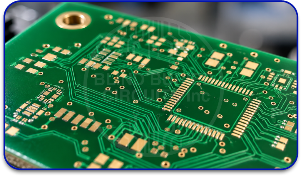
PCB solder mask is the same protective layer, and “solder mask” is the term most common in the United States. It is the thin, lacquer-like coating that gives a circuit board its familiar color. On a finished circuit board, the solder mask covers the traces and leaves the pads open for component soldering.
The openings in a circuit board solder mask are defined by a dedicated solder mask layer in the design data, which is supplied to the fabricator with the Gerber files. Where fine-pitch components are used, a narrow strip of mask between adjacent pads, called a solder mask dam, helps keep solder from bridging.
How to Choose the Right Solder Resist or Solder Mask for Your PCB
The right PCB solder mask material depends on your board design, how it will be assembled, and where it will be used.
- Board type: Rigid, flex, rigid-flex, and HDI boards each have different needs. For fine-pitch parts and BGA solder mask designs, check opening clearances and registration so pads stay uncovered.
- Flexibility: Use polyimide coverlay where the circuit bends repeatedly. Flex PCB solder mask works in areas with limited or static bending.
- Compatibility: Make sure the PCB solder resist works with your surface finish, soldering process, cleaning chemicals, and operating temperature.
- Fabricator capability: Confirm minimum mask openings, registration tolerance, and dam width before finalizing the circuit board solder mask layer.
- Pads and vias: State which ones stay exposed, tented, plugged, or filled. Blind vias need a defined treatment, while buried vias need no mask opening.
Solder Resist vs. Solder Mask: Is There Any Difference?
No. PCB solder resist and PCB solder mask are two names for the same coating. They do the same job, use the same materials, and are applied by the same processes. The difference is only in terminology, which varies by region, company, and document. You may also see “solder stop” or “solder stop mask” in some drawings and specifications.
Two related terms are easy to confuse with it:
- Peelable solder mask: This is a temporary coating that is removed after a process step, such as selective soldering or plating. Permanent solder resist or solder mask stays on the board for its entire life.
- Solder paste layer: This is a separate design layer that defines where solder paste is applied through a stencil. It is not the protective coating itself.
How Is Solder Resist or Solder Mask Applied to a Circuit Board?
The process depends on the PCB solder mask material and the fabrication method. A typical liquid photoimageable (LPI) process runs in six steps:
- Surface preparation: The copper is cleaned by brushing, pumice scrubbing, or microetching, then dried, so the PCB solder resist bonds well.
- Mask application: LPI is applied by curtain coating, spray coating, or screen printing. Dry-film mask is laminated on, and inkjet printing deposits UV-curable ink droplets directly onto the board.
- Pre-curing: The coating is tack-dried in an oven so it holds its shape but stays photosensitive for imaging.
- UV exposure and imaging: A phototool or laser direct imaging (LDI) system defines the pattern, aligned to the board’s fiducials. UV light hardens the exposed areas.
- Development: A soda ash solution washes away the unexposed mask, opening the pads and features needed for assembly.
- Final curing and inspection: Thermal curing, sometimes with UV, completes the circuit board solder mask. Automated optical inspection (AOI) then checks coverage and pad clearance, and the exposed pads receive their surface finish.
Non-photoimageable and selectively printed systems use different patterning and curing methods.
Solder Resist Materials Used in PCB Fabrication
PCB solder mask material is a polymer-based formulation selected for adhesion, thermal stability, chemical resistance, and electrical insulation. The table below summarizes the main materials and components used in rigid and flexible boards.
| Material | Key Role | Typical Use |
|---|---|---|
| Epoxy-based resin | Insulation, adhesion, heat and chemical resistance | Rigid PCBs |
| Epoxy-acrylate hybrid | Heat resistance plus photoimaging for fine patterns | LPI mask, fine-pitch and HDI boards |
| Additives (photoinitiators, fillers, pigments) | Control curing, finish, and color | All mask types |
| Polyimide coverlay | Withstands repeated bending | Flex and rigid-flex bend areas |
| Flexible solder mask | Fine openings with some flexibility | Flex PCB areas with limited or static bending |
Whichever material is used, a good PCB solder mask material should withstand PCB assembly temperatures, resist the fluxes and cleaning chemicals used in soldering, stay adhered to the laminate and copper, and keep its insulating properties over the life of the product.
Types of PCB Solder Resist and Solder Mask
Solder mask types describe the material form, while spraying, curtain coating, screen printing, lamination, and inkjet printing describe how the mask is applied. The common types are:
- Liquid photoimageable (LPI) solder mask: The most widely used type. The liquid is coated onto the board, exposed to UV light, and developed to open pads and features. It supports fine patterns, which makes it the standard choice for multilayer and high-density PCBs.
- Dry-film photoimageable solder mask: Supplied as a solid film that is laminated onto the PCB, then imaged and developed. It provides controlled film thickness and may support specific via-tenting applications, but coverage over raised copper features depends on lamination conditions and board topography.
- Epoxy screen-printed solder mask: The mask is deposited through a screen and then cured, so the pattern is defined by the screen. Resolution is lower than LPI, so it is generally used for simpler boards with coarser features.
- Inkjet solder mask: UV-curable ink is printed directly onto the board from digital data, without a phototool. It is commonly used for prototypes, short runs, and designs that change often.
What Are the Popular PCB Solder Mask Colors?
PCB solder mask is available in several colors, with differences mainly in appearance, visual inspection, and specific application needs.
- Green: The most widely used PCB solder mask color, supported by established manufacturing processes and familiar inspection settings. It generally provides good contrast for exposed copper, solder pads, and white legend markings.
- Blue: It is commonly selected for development boards and consumer electronics where visual differentiation is desired. Its suitability for fine features depends on the specific mask formulation and the manufacturer’s process capabilities.
- Red: This color is often chosen for product identification, prototypes, and distinctive board designs. As with other colors, achievable mask resolution and inspection performance depend on the material and fabrication process.
- Black: It is used when a dark, uniform board appearance is preferred. Its lower visual contrast with some dark features can make manual inspection and defect identification more challenging.
- White: A white-colored circuit board mask is used in LED lighting applications because it can provide a reflective surface. The actual reflectance depends on the formulation, and discoloration or contamination may be more noticeable.
- Yellow and other specialty colors: Yellow, purple, and similar options are available from some fabricators, often for visual differentiation or product identification. Availability and design capabilities vary by supplier.
Applications of PCB Solder Mask: Standard, BGA, Flex, and Blind Buried Via PCBs
The role of PCB solder mask varies according to board construction, component layout, and via design.
- Standard Rigid PCBs: Circuit board solder mask covers most exposed copper traces while leaving designated solder pads, test points, and connector contacts accessible. It helps reduce solder bridging and protects copper from oxidation and environmental contamination.
- BGA Solder Mask Design: BGA solder mask designs commonly use solder mask defined (SMD) or non-solder mask defined (NSMD) pads. SMD openings are smaller than the copper pads, allowing the mask to overlap their edges. NSMD openings are larger, leaving the pad perimeter exposed. Selection depends on component recommendations and fabrication capabilities.
- Flex PCB Solder Mask: Flex PCB solder mask may be suitable for flexible circuits where bending requirements are limited and the material supports the intended movement. Polyimide coverlay, a flexible film bonded with adhesive, is commonly used in areas subject to repeated bending.
- Blind and Buried Via PCBs: Blind vias connect an external layer to one or more internal layers and reach a board surface. Their openings may be exposed or covered according to design requirements. Buried vias connect internal layers without reaching an external surface, so they do not require direct solder mask openings.
Common Solder Resist and Solder Mask Defects and How to Prevent Them
Defects in PCB solder resist can affect solderability, copper protection, and long-term reliability, especially on fine-pitch and BGA solder mask designs. Most can be avoided with good process control and a DFM review.
| Defect | Common Cause | How to Prevent It |
|---|---|---|
| Misregistration | Imaging errors, tight pad clearances | Check mask-to-copper registration and confirm tolerances in the DFM review |
| Pinholes and voids | Contamination, trapped air, uneven coating | Clean the surface well, control coating, and inspect |
| Incomplete curing | Wrong oven temperature or time | Follow the PCB solder mask material’s curing profile |
| Peeling and blistering | Poor cleaning, trapped moisture, thermal stress | Clean and dry thoroughly and use compatible materials |
| Slivers and dam breakdown | Very narrow mask dams between fine-pitch pads | Confirm minimum dam width with the fabricator and adjust pad spacing or openings |
Why Choose Blind Buried Circuits for Your PCB?
Planning a multilayer PCB with blind and buried vias? Blind Buried Circuits works with your design before it reaches the production floor, so solder mask and fabrication issues are caught early.
- Engineering review of your files: Share your Gerber files, layer stack-up, and via specifications, and our engineers check them against our manufacturing capabilities.
- Solder mask clearances and registration: We review mask openings, dam widths, and registration requirements, especially for fine-pitch, BGA, and via-dense boards.
- Blind and buried via expertise: We confirm how blind vias should be treated (exposed, tented, plugged, or filled), and we help you avoid fabrication constraints in complex multilayer builds.
- Clear quote and next steps: Send us your PCB specifications and we will respond with a manufacturing quote.
Talk to Blind Buried Circuits today. Share your Gerber files, stack-up, and via specifications to request a manufacturing quote.