

Objective
This guide explains what peelable solder mask is, where it is used, and how to apply, remove, and choose one for your PCB process.
Key Takeaways
- Peelable solder mask is a temporary coating that covers selected PCB areas during a process and is peeled off afterward. A permanent solder mask stays on the board.
- It is commonly used in wave soldering, through-hole assembly, and conformal coating, and to protect gold fingers and connector contacts.
- Peelable mask suits irregular shapes, while high-temperature tape suits simple, flat areas.
- Temperature, chemical resistance, cure time, and removal vary by product, so always check the technical data sheet.
- Cure the mask fully, and peel it at the stage the instructions recommend, to avoid tearing and residue.
Table Of Contents
-
-
- Introduction
- What Is Peelable Solder Mask in PCB Manufacturing?
- Why Use Peelable Solder Mask? Key Benefits
- Where Is Peelable Solder Mask Used? Common PCB Applications
- Peelable Solder Mask vs. Permanent Solder Mask: What Is the Difference?
- Peelable Solder Mask vs. High-Temperature Tape and Other Masking Methods
- How to Apply and Remove Peelable Mask in PCB Manufacturing
- Peelable Solder Mask Design Guidelines for PCB Designers
- Common Peelable Solder Mask Problems and How to Fix Them
- Why Choose Blind Buried Circuits for Your Peelable Solder Mask Needs?
- Frequently Asked Questions
-
Introduction
In printed circuit board (PCB) manufacturing, protecting specific areas of a circuit board during soldering and coating processes is essential for maintaining quality and reliability. Peelable and permanent solder masks play important roles in PCB production, each serving different purposes. Peelable solder masks offer flexibility in manufacturing, making them a useful option for specific PCB requirements. Choosing the right masking solution is important for achieving reliable results. This post explores what peelable solder mask is, its benefits, applications, and key selection considerations in PCB manufacturing.
What Is Peelable Solder Mask in PCB Manufacturing?
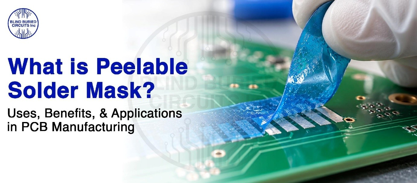
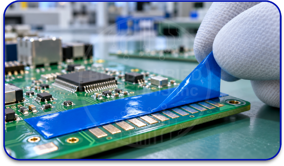
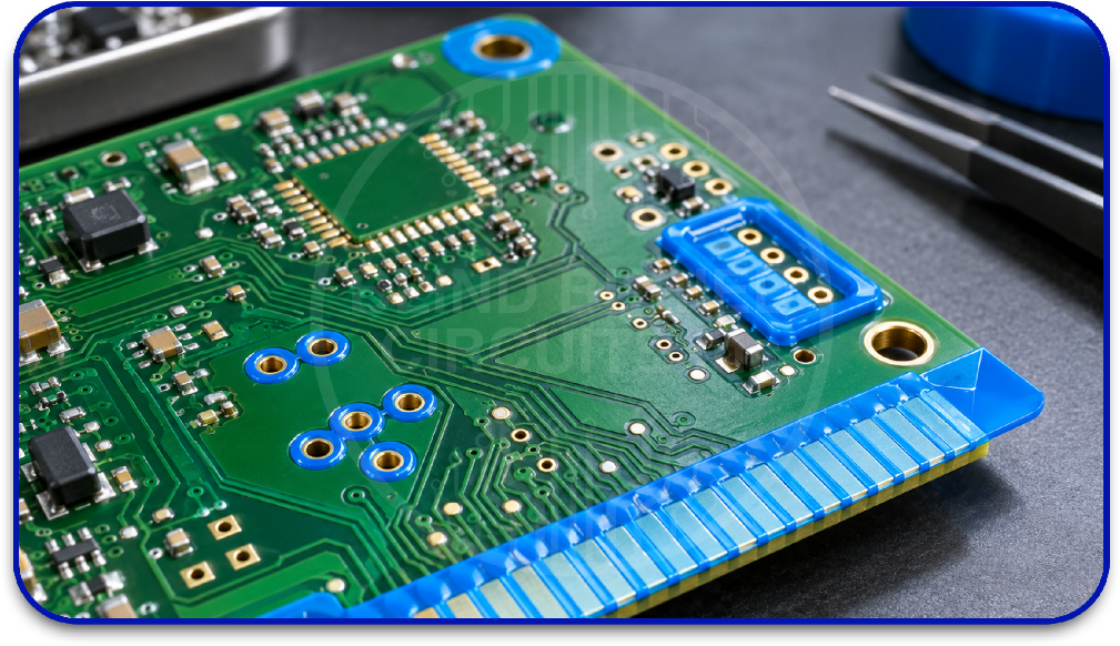
A peelable solder mask is a temporary coating that protects selected areas of a printed circuit board (PCB) during soldering or conformal coating, and then peels off by hand. It is also called a peelable mask, strippable mask, or temporary solder mask. Unlike a permanent solder mask, it does not stay on the finished board.
Peelable solder mask PCB products are usually applied as a liquid that cures into a flexible film. Many are blue, but color varies by product.
A peelable mask in PCB work is typically used to:
- Keep solder off gold fingers, connector contacts, and other areas that must stay clean
- Cover selected areas during wave soldering
- Block conformal coating from connectors, switches, and test points
Why Use Peelable Solder Mask? Key Benefits
A peelable solder mask is a temporary coating. You apply it over the areas of a board you want to protect, finish the process, and peel it off. Here is why it is used in PCB manufacturing and assembly.
Easy to remove: Permanent solder mask stays on the board for life, while a peelable mask in PCB work usually comes off by hand when the job is done. This works best when the mask is applied and cured correctly.
Handles soldering heat: Many peelable masks are made to hold up during soldering, including wave soldering. Temperature limits differ from product to product, so check the data sheet before you choose one.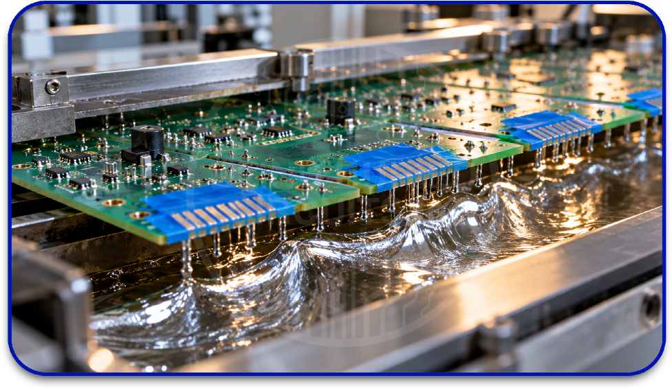
Resists process chemicals: The mask can shield covered areas from fluxes and cleaning agents. Not every peelable solder mask PCB product suits plating or harsh chemicals, so test it against your own process.
Protects only what you choose: You can cover connector contacts, gold fingers, or holes and leave the rest of the board open for soldering or coating.
Means less rework: When the mask is applied correctly, solder and coatings stay out of protected areas. That saves cleanup time later.
Where Is Peelable Solder Mask Used? Common PCB Applications
A peelable solder mask goes on during a specific process step and comes off afterward. These are the most common places it is used:
- Wave soldering: The underside of the board passes over molten solder. A peelable mask covers gold fingers and contacts that must stay free of solder.
- Through-hole assembly: It covers selected areas while component leads are soldered. Keep the mask clear of the holes and pads you want to solder, so it does not block solder flow.
- Conformal coating: Compatible temporary peelable masks can protect selected connectors, contacts, and test points from conformal coating. The masking material and removal procedure must be validated for the coating process to avoid residue or damage to coating edges.
- Connector contacts and gold fingers: It keeps solder and coating off edge connectors and contact surfaces, so electrical contact and fit stay intact.
Peelable masks in PCB work are also useful on boards that mix connectors, components, and exposed contacts that need different treatment. Because each product has different limits, check the technical data sheet for temperature resistance, curing conditions, compatibility, and removal steps before using a peelable solder mask PCB product.
Peelable Solder Mask vs. Permanent Solder Mask: What Is the Difference?
Both are used in PCB manufacturing, but they do different jobs. A permanent solder mask stays on the board for life, while a peelable solder mask is a temporary coating that is removed after a process step.
| Feature | Permanent Solder Mask | Peelable Solder Mask |
|---|---|---|
| Main purpose | Insulates copper and prevents solder bridging | Temporarily covers selected areas during a process |
| When it is applied | During PCB fabrication | During fabrication or PCB assembly, when temporary protection is needed |
| How it is applied | Coating, imaging, and curing | Dispensing, brushing, or another method the manufacturer approves |
| Curing | Controlled curing after imaging | Depends on the formulation |
| Removal | Stays on the finished board, and removing it can damage the surface | Peels off as a layer after the process |
| What it must withstand | Long-term insulation and environmental protection | Process heat and chemicals while staying easy to remove |
Peelable Solder Mask vs. High-Temperature Tape and Other Masking Methods
A peelable solder mask and high-temperature tape both cover areas of a PCB temporarily. The better choice depends on the board’s shape, the process, and how fast you need to mask and unmask.
- Application: A peelable solder mask is applied as a liquid or paste and left to cure. Tape is a ready-made adhesive strip or sheet, so it is quick to place on flat, easy-to-reach areas.
- Coverage: Peelable mask fits odd shapes and tight spaces, but clean edges depend on your technique. Tape gives sharp edges but is hard to fit around complex or closely spaced features.
- Heat resistance: The mask must hold up through the process temperature. Tape must handle the heat without its adhesive failing.
- Chemical resistance: Both vary by product, so test them against your own fluxes, cleaners, and coating chemicals.
- Removal: Peelable mask comes off as one layer. Tape also peels off, but heat can leave adhesive residue.
- Best use: A peelable mask in PCB work suits irregular areas and selective masking. Tape suits simple jobs where fast placement matters.
How to Apply and Remove Peelable Mask in PCB Manufacturing
Follow the manufacturer’s technical data sheet (TDS) for application, curing, and removal. These six steps show how a peelable solder mask is used from start to finish.
- Prepare the surface: Mark the areas to protect, such as gold fingers, connector contacts, and holes that must stay free of solder. Clean off dust, oils, and contaminants with a PCB-safe method, then dry the board.
- Apply the mask: Apply the peelable solder mask PCB coating by hand or with compatible dispensing equipment. Cover the area fully, with no gaps or pinholes, and keep it off surfaces you want exposed.
- Cure it: Follow the cure time and temperature on the data sheet. A dry-to-touch surface is not always fully cured.
- Run your process: Continue with wave soldering or conformal coating. Confirm the mask handles your process heat, fluxes, cleaners, and coating materials.
- Remove the mask: Peel it off at the stage the product instructions recommend. For conformal coating, good timing gives clean coating edges and avoids damage.
- Inspect: Check contacts, gold fingers, and holes for mask residue, stray solder, or coating. If cleaning is needed, use a method that is safe for the assembly.
Peelable Solder Mask Design Guidelines for PCB Designers
Clear masking notes in your design files help the fabricator and assembler apply a peelable solder mask correctly. Follow these five guidelines:
- Mark the masking areas: Identify contacts, gold fingers, and any holes or pads that must stay free of solder or coating. Show them clearly in your fabrication or PCB assembly documentation.
- Leave room around the area: Keep enough space around components and nearby features so the mask can go on and come off without damaging solder joints or coatings.
- Specify thickness and curing: Confirm the mask thickness, application method, and curing conditions with your material supplier and PCB manufacturer.
- Specify masking boundaries: Clearly identify areas requiring temporary protection and confirm that the mask can be applied and removed without affecting adjacent components, pads, or coatings.
- Match the mask to your process: Make sure the peelable mask handles your soldering or coating temperature and the chemicals it will be exposed to.
Common Peelable Solder Mask Problems and How to Fix Them
Application and removal issues can affect masking performance and PCB assembly quality. The following problems should be addressed through process checks and manufacturer guidance.
- Incomplete Curing: The mask may not withstand processing or peel cleanly. Follow the specified curing time and temperature, accounting for application thickness.
- Mask Tearing During Removal: Thin coverage or unsuitable removal conditions may cause the mask to break. Verify application thickness and follow the recommended removal procedure.
- Residue on PCB Surfaces: Residue may result from incompatible materials or improper curing. Check product compatibility and use only manufacturer-approved cleaning methods.
- Accidental Coverage: Mask may spread onto contacts, solder joints, or areas intended to remain exposed. Improve application control and inspect masking boundaries before curing.
- Poor Process Resistance: The mask may degrade during soldering or chemical exposure. Confirm temperature limits and chemical compatibility using the product’s technical data sheet before production.
Why Choose Blind Buried Circuits for Your Peelable Solder Mask Needs?
Before you finalize your PCB manufacturing process, make sure your peelable solder mask suits your board. Blind Buried Circuits checks this with you, so masking problems are found before production begins.
- Design and assembly review: Share your PCB design files and assembly requirements with our engineering team, and we will review your masking areas.
- Process compatibility check: We confirm the peelable mask works with your soldering or conformal coating process, including temperature, chemical resistance, application, and removal needs.
- Early issue spotting: We identify possible process problems before they reach the production floor.
- The right masking solution: We help you decide on the most suitable masking method for your production needs.
Request a peelable solder mask compatibility review from Blind Buried Circuits today. Send us your design files and assembly requirements to get started.