

Objective
To explain how PCB stackup design affects signal integrity, impedance control, routing, and manufacturability, and how to develop a reliable stackup for high-speed PCB applications.
Key Takeaways
- Understand what a PCB stackup is and how signal, power, ground, and dielectric layers work together.
- Learn how stackup geometry affects impedance, signal-return paths, crosstalk, and power integrity.
- Understand how to select the appropriate layer count, materials, dielectric thickness, and reference-plane arrangement.
- Learn practical PCB stacking techniques for high-speed signal integrity and manufacturability.
- Identify common stackup design mistakes and understand why manufacturer review should happen before routing begins.
Table Of Contents
- Introduction
- What Is a PCB Stackup?
- Understanding the Layers in a PCB Stackup
- Why PCB Stackup Design Matters for High-Speed Signals?
- How to Choose the Right PCB Layer Stackup for High-Speed Signals?
- PCB Stacking Techniques for Signal Integrity
- How to Design a PCB Stackup for High-Speed Signals
- Tools and Techniques for PCB Stackup Planning
- Common PCB Stackup Design Mistakes to Avoid
- PCB Stackup Design and Manufacturing Considerations
- Why Choose Blind Buried Circuits for PCB Stackup Design?
- Frequently Asked Questions
Introduction
A PCB stackup defines the number, order, and construction of copper and dielectric layers within a multilayer PCB, including the arrangement of signal layers, reference planes, power planes, cores, and prepregs. In high-speed PCB designs, this layer structure directly influences controlled impedance, signal-return paths, crosstalk, power integrity, and electromagnetic behaviour.
As signal speeds and routing density increase, an unsuitable PCB layer stackup can make impedance control more difficult, disrupt return-current paths, increase unwanted coupling, and create manufacturing constraints. Layer count alone does not determine whether a stackup is suitable; dielectric thickness, material properties, copper thickness, reference-plane placement, via structures, board thickness, and fabrication capabilities must be considered together.
This guide explains how to develop a reliable PCB stackup for high-speed signals, including layer selection, dielectric construction, impedance control, reference-plane arrangement, routing considerations, and manufacturability. It also explains when 4-layer, 6-layer, and 8-layer PCB stackups may be appropriate and why the proposed stackup should be reviewed with the PCB manufacturer before detailed routing begins.
What Is a PCB Stackup?
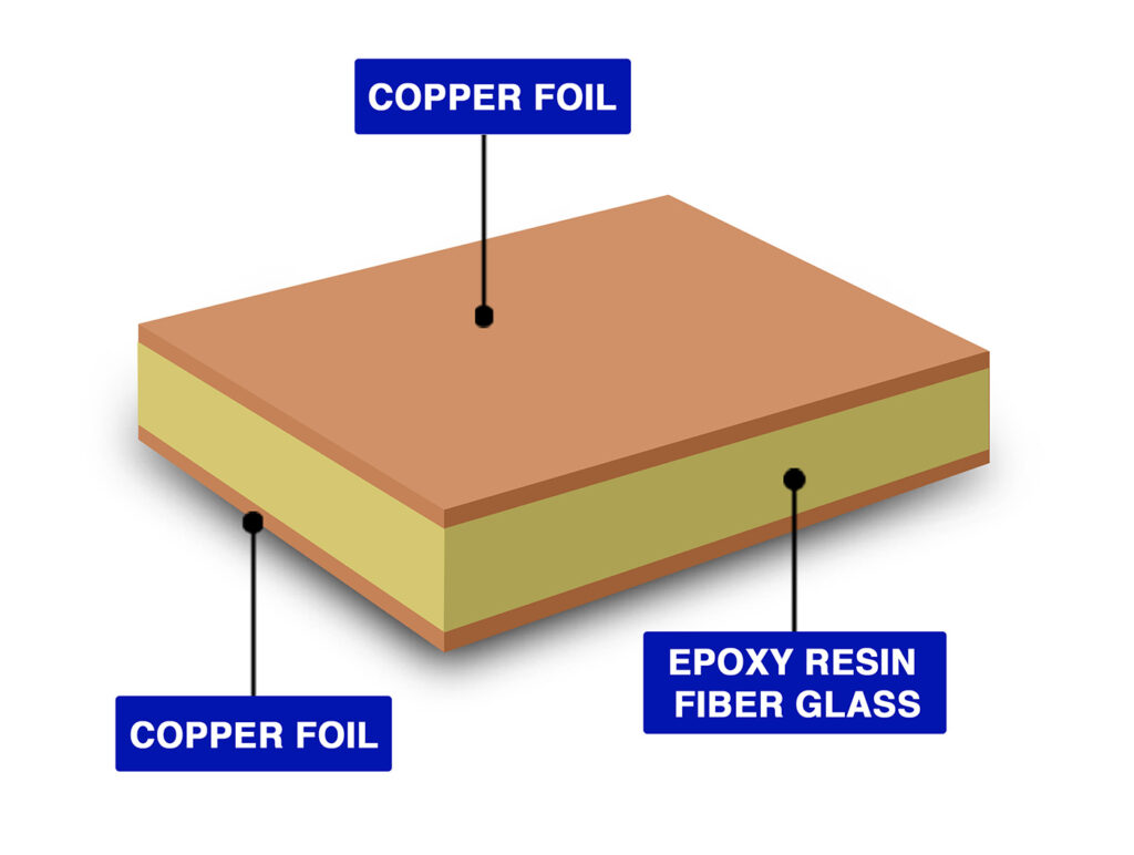
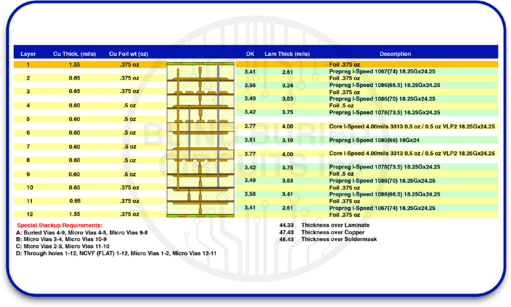
A PCB stackup is the defined arrangement of conductive copper layers and insulating dielectric layers within a multilayer printed circuit board. It specifies the number, sequence, and construction of these layers, including signal, power, and reference-plane layers. The stackup also establishes the physical relationships between adjacent layers, which determine factors such as dielectric thickness, copper distribution, and overall board thickness. A controlled stackup provides the structural framework needed to manufacture the PCB consistently according to its electrical, mechanical, and fabrication requirements.
Understanding the Layers in a PCB Stackup
A multilayer PCB stackup consists of conductive and dielectric layers, each serving a distinct electrical or structural function.
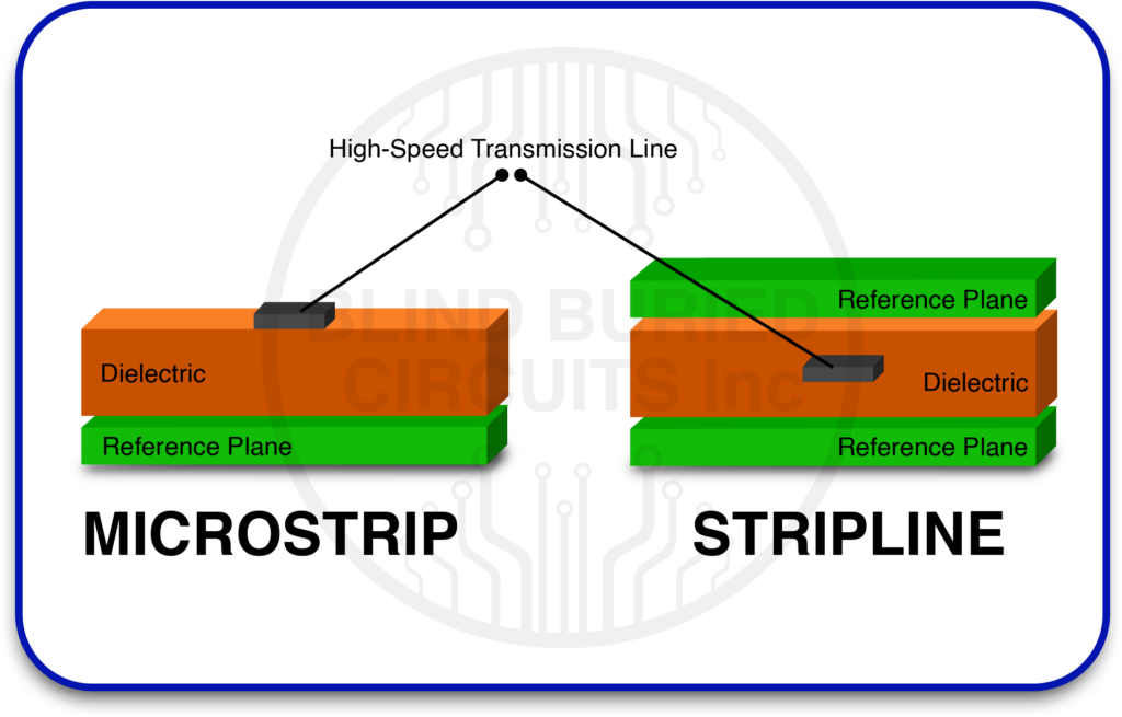
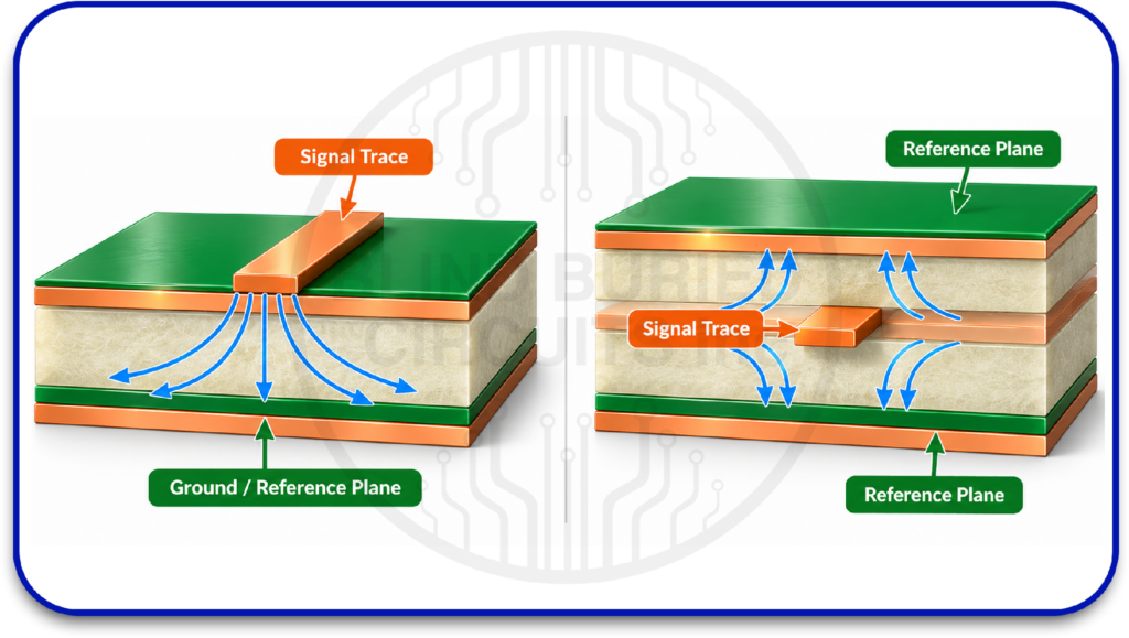
Signal Layers: Signal layers carry routed electrical signals between components and interconnects. Depending on their position relative to reference planes, they can form microstrip structures on outer layers or strapline structures on inner layers.
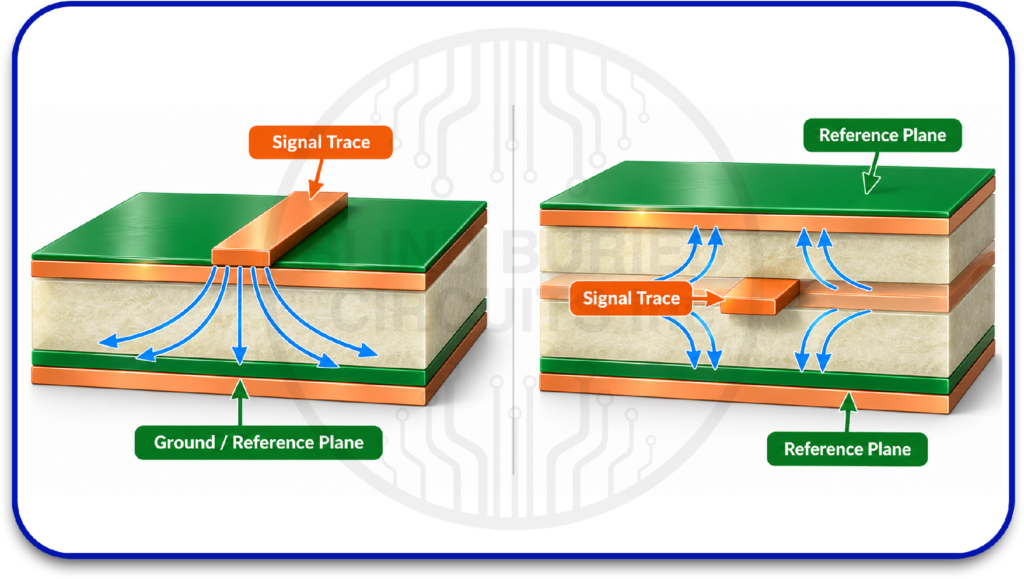
Ground and Reference Planes: Ground and reference planes provide stable reference structures for signal transmission and low-inductance return-current paths. Their continuity is particularly important for high-speed interconnects.
Power Planes: Power planes distribute supply voltages across the PCB and form part of the power-distribution network. Depending on the stackup, they may also serve as reference structures for adjacent signal layers.
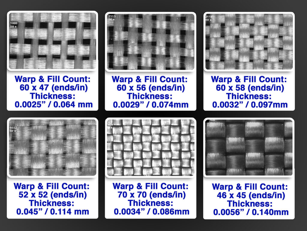
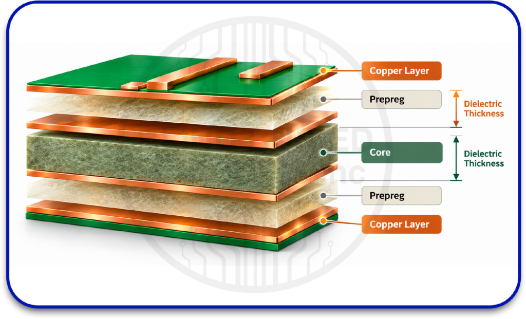
Core and Prepreg Dielectrics: Core and prepreg materials electrically separate conductive layers and provide mechanical insulation within the board. Their dielectric properties and thickness influence impedance, propagation characteristics, and the geometry of controlled-impedance structures.
Why PCB Stackup Design Matters for High-Speed Signals?
For high-speed PCBs, the stackup establishes the physical and dielectric environment in which signals propagate. The arrangement of conductive layers, reference planes, and dielectric materials affects several aspects of electrical and mechanical performance.
- Controlled Impedance: Trace geometry and its relationship to adjacent reference planes determine characteristic impedance. Consistent layer spacing and dielectric properties help maintain predictable impedance along controlled-impedance interconnects.
- Predictable Signal-Return Paths: The position and continuity of reference planes influence the path taken by high-frequency return currents. A suitable layer arrangement helps maintain a continuous, low impedance return path.
- Crosstalk Control: The spacing between signal layers and neighboring conductors affects electromagnetic coupling. Stackup geometry therefore influences the amount of capacitive and inductive coupling between adjacent interconnects.
- Power Integrity: Power and reference-plane arrangement affect the geometry and impedance of the power-distribution network. The stackup can therefore influence voltage fluctuations, transient behavior, and plane-related resonances.
- EMI Management: Signal and reference-layer relationships affect electromagnetic field distribution and current-loop areas. A well-defined stackup can help control unintended radiation and susceptibility to external electromagnetic fields.
- Mechanical Symmetry and Manufacturability: Balanced layer construction can help reduce mechanical stress and minimize board warpage during fabrication and PCB assembly. Consistent dielectric and copper distribution also supports more predictable manufacturing results.
How to Choose the Right PCB Layer Stackup for High-Speed Signals?
The right high-speed PCB stackup depends on the electrical and physical requirements of the application rather than a fixed number of layers. Consider the following factors when determining the appropriate stackup architecture.
- Signal and Routing Requirements: Assess the number, type, and density of high-speed interfaces, including differential pairs, buses, clocks, and other constrained signals. The stackup must provide sufficient routing capacity without compromising required signal paths.
- Impedance Requirements: Establish the required single-ended and differential impedance targets for controlled-impedance interfaces. The stackup must provide suitable conductor-to-reference-plane relationships for achieving those targets.
- Reference-Plane Requirements: Determine which signal layers require dedicated or suitable reference planes. High-speed interfaces benefit from consistent reference structures that support predictable electromagnetic behavior and return-current continuity.
- Layer Count and Board Density: Select the layer count according to routing density, component technology, board dimensions, power-distribution requirements, and reference-plane needs. A 4-layer PCB stackup, 6-layer PCB stackup, or 8-layer PCB stackup may each be appropriate depending on the application.
- Electrical and Mechanical Requirements: Consider power-distribution needs, finished board thickness, copper distribution, thermal requirements, and mechanical constraints alongside signal-routing requirements. The stackup must satisfy these requirements as an integrated board structure.
PCB Stacking Techniques for Signal Integrity
Effective PCB stacking techniques establish predictable electrical relationships between signal layers, reference planes, and dielectric materials, supporting controlled impedance, return-current continuity, and reduced electromagnetic coupling.
- Keep High-Speed Signal Layers Close to Reference Planes: Placing high-speed signal layers close to continuous reference planes helps maintain predictable transmission-line characteristics and provides a shorter, lower-inductance return-current path.
- Use Appropriate Plane Pairing: Arrange power and reference planes to support effective power distribution and appropriate high-frequency current paths. Plane spacing also influences the electrical behavior of the power-distribution network.
- Maintain Stackup Symmetry: Balanced layer constructions help distribute mechanical stresses more evenly during lamination and thermal processing, reducing the risk of board warpage.
- Separate Sensitive Signal Environments: Use layer arrangement, reference planes, and adequate spacing to reduce unwanted electromagnetic coupling between sensitive circuits and higher-noise signal environments.
- Control Dielectric Geometry: Select dielectric thickness and material properties together with trace width and copper thickness to achieve the required impedance while maintaining practical fabrication tolerances.
How to Design a PCB Stackup for High-Speed Signals
Once the stackup requirements are established, the design process translates them into a manufacturable layer structure.
- Establish the Layer Sequence: Define the order of signal, reference, and power layers so that critical signals have appropriate electromagnetic reference structures and practical routing paths.
- Define Dielectric Construction: Select core and prepreg constructions and establish the dielectric thicknesses between conductive layers. These dimensions become part of the electrical geometry of controlled-impedance structures.
- Establish Conductor Geometry: Determine trace widths, copper thicknesses, and spacing required to achieve the specified impedance targets. Field-solver or stackup-design calculations can be used to evaluate the resulting transmission-line geometry.
- Plan Layer Transitions: Determine how signals will move between layers and select suitable via structures. Evaluate via inductance, capacitance, stubs, and manufacturability where they are relevant to the interface.
- Check Power and Reference Structures: Review the completed layer arrangement to confirm that power-distribution and reference structures are physically compatible with the intended routing and electrical requirements.
- Validate the Proposed Stackup: Review the complete construction with the PCB fabricator, confirming material availability, dielectric tolerances, copper thicknesses, via capabilities, finished thickness, and impedance-control capability before routing begins.
Tools and Techniques for PCB Stackup Planning
PCB stackup planning uses a combination of calculation, simulation, and documentation tools to evaluate electrical relationships before layout begins.
- Stackup Planning Software: Use dedicated stackup tools to model layer structures, dielectric constructions, copper thicknesses, and conductor geometry in a single design environment.
- Field-Solver Analysis: Use 2D electromagnetic field solvers to calculate transmission-line characteristics and evaluate how conductor geometry and surrounding materials affect impedance.
- Impedance Calculators: Calculate preliminary single-ended and differential impedance values to establish practical trace geometries before detailed routing.
- Material Libraries: Use appropriate laminate data for the intended calculation or field solver, including dielectric properties, loss characteristics and thickness information. Where controlled impedance or high-speed loss performance is critical, confirm that the Dk/Df values and test conditions used are appropriate for the design and frequency range.
- Stackup Documentation: Document layer order, material construction, copper weights, dielectric dimensions, impedance targets, and relevant tolerances so the intended construction is clearly communicated.
- Design Rule Checks: Apply stackup-related design rules to identify incompatible geometries, spacing conditions, or layer assignments before the PCB layout is finalized.
Common PCB Stackup Design Mistakes to Avoid
Several stackup decisions can create avoidable electrical or manufacturing problems:
- Ignoring dielectric tolerances: Nominal dielectric thickness may differ from the manufactured value, affecting controlled impedance.
- Insufficient reference-plane continuity: High-speed signals without suitable reference structures can develop unpredictable return-current paths.
- Unbalanced copper distribution: Significant asymmetry can increase the risk of board warpage during fabrication.
- Overlooking via structures: Via stubs and layer transitions can introduce discontinuities in high-speed signal paths.
- Choosing materials without fabrication verification: A theoretically suitable stackup may not be practical with the manufacturer’s available materials and processes.
- Adding layers without a defined requirement: Higher layer count does not inherently improve signal integrity or electrical performance.
PCB Stackup Design and Manufacturing Considerations
A high-speed PCB stackup must account for both electrical requirements and fabrication capabilities.
- Material Availability: Confirm suitable core and prepreg constructions, dielectric properties, and available copper weights.
- Dielectric Tolerances: Account for variations in dielectric thickness and material properties that can affect controlled impedance.
- Board Construction: Consider finished thickness, copper distribution, and layer registration requirements.
- Via Technology: Verify the manufacturer’s capabilities for through-holes, blind and buried vias, and microvias where applicable, including relevant aspect-ratio, drilling, registration and sequential-lamination constraints.
- Fabrication Verification: Review the proposed stackup and impedance requirements with the PCB manufacturer before routing to ensure the intended construction is manufacturable within specified tolerances.
Why Choose Blind Buried Circuits for PCB Stackup Design?
At Blind Buried Circuits, we work with customers to translate electrical and mechanical requirements into practical PCB stackup constructions. We can review layer configurations, material combinations, impedance requirements, and fabrication constraints to help establish a stackup that is suitable for the intended application and manufacturing process.