Objective
You want a flex or rigid-flex board that builds cleanly, assembles well, and survives bending. This guide explains practical DFM steps for SMT builds, with simple rules you can apply before you release files.
Key Takeaways
- Flex and rigid-flex boards move and stretch during heat. That can break solder joints if you place parts in the wrong spot.
- Rigid-flex PCB design rules are mostly about managing stress, heat, and stackup changes.
- Good pad, coverlay, and routing choices prevent common SMT defects like tombstoning and wicking.
- Stiffeners and carriers are not optional for many flex SMT jobs. They are part of DFM.
- Early DFM reviews reduce scrap and speed up the first-pass build.

Table of Contents
- Why DFM matters for flex and rigid-flex
- Flex and rigid-flex basics
- SMT assembly challenges
- Stackup and material DFM guidelines
- SMT placement rules
- Pads, coverlay, and via decisions
- Routing and via DFM rules
- Stiffeners and support structures
- DFM rules for the SMT process
- Inspection and test planning
- Common DFM mistakes and how to avoid them
- Designer–manufacturer teamwork
- Benefits of strong DFM
- Conclusion and FAQs
1) Introduction: Why DFM Is Critical for Flex and Rigid-Flex PCBs
Flex and rigid-flex PCBs are everywhere now. You see them in phones, cameras, cars, and medical gear. They save space and reduce connectors. But they are harder to build than rigid boards.
Here is the key issue. Flex materials can warp during reflow. Rigid-flex has transition zones that can crack if the design is not careful. That is why DFM matters.
If you follow Blind Buried Circuits, you already know the goal is not just “it works on a screen.” The goal is “it builds the same way every time.”
Did you know facts
- Flex circuits often use polyimide because it stays stable at higher heat than many plastics.
- Rolled copper bends better than some other copper types because it handles repeated flexing with less cracking.
Many rigid-flex failures happen near the rigid-to-flex transition because that is where stress concentrates.

2) Understanding Flex and Rigid-Flex PCB Technology
What Is a Flex PCB
A flex PCB is a circuit on a flexible base, often polyimide. It can be single-layer or multilayer.
Single-layer flex is simpler and cheaper.
Multilayer flex supports more routing, but needs tighter process control.
What Is a Rigid-Flex PCB
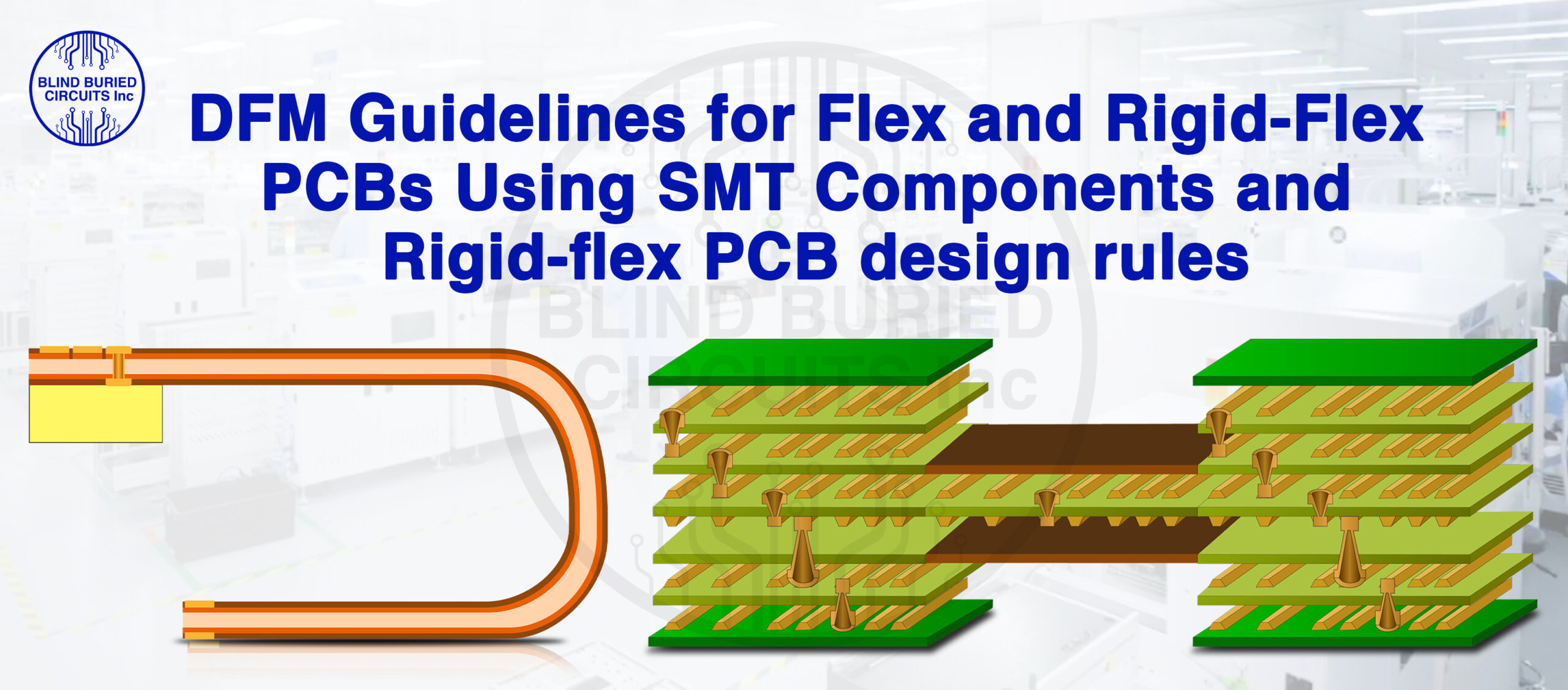
A rigid-flex PCB combines rigid sections with flexible sections in one board. It lets you fold the board into a shape.
Typical uses include:
- Hinged or folded products
- Space-limited enclosures
- Designs that replace cable assemblies
How flex differs from rigid in manufacturing
Flex materials expand and relax more during lamination and reflow. Flex also bends, which creates mechanical fatigue over time.
Here is a quick comparison:
| Topic | Rigid PCB | Flex / Rigid-Flex |
| Reflow behavior | More stable | Higher warpage risk |
| Handling | Easy | Often needs carriers |
| Long-term stress | Mostly vibration | Vibration plus bending |
| Common failures | shorts/opens | solder fatigue, cracks |

3) SMT Assembly Challenges in Flex and Rigid-Flex PCBs
Material stability during SMT reflow
Flex stacks can expand at different rates than copper. That can cause:
- Warpage during reflow
- Skew during pick-and-place
- Uneven solder wetting
Component support and handling
Flex areas do not have stiffness. That makes accurate placement harder.
Common DFM supports are:
- Temporary carriers
- Pallets
- Stiffeners bonded to the flex
Yield risks unique to flex SMT
Watch for:
- Solder joint cracking after bend cycles
- Misalignment from board movement
- Pad lifting if coverlay openings are wrong
4) Stackup and Material Selection DFM Guidelines
Choosing the right flex materials
Start with thickness. Thinner flex bends better, but can move more during reflow.
Also decide between:
- Adhesive-based laminates (often easier to source, but can add thickness)
- Adhesiveless laminates (often better for fine features and bending)
Copper type and thickness
Copper choice affects bend life.
General DFM guidance:
- Use copper thickness that meets current needs without over-stiffening the bend
- Prefer bend-friendly copper in dynamic flex zones
Rigid-flex transition zone design rules
This is a core part of Rigid-flex PCB design rules.
Do these things:
- Avoid abrupt stackup changes at the transition
- Use smooth coverlay and dielectric tapers where possible
- Keep plated features away from the bend and transition edge
5) SMT Component Placement Guidelines
SMT parts should usually sit on rigid areas. Flex zones move. Movement stresses solder joints.
Component placement in rigid vs flex areas
Best practice:
- Place SMT in rigid zones
- Place connectors and heavy parts on rigid areas with stiffeners
Exceptions can work, but only with strict control.
Keep-out zones near bend areas
A simple rule is: keep components away from bend lines. The exact distance depends on thickness and bend radius.
Practical DFM tips:
- Keep parts, vias, and pads out of dynamic bend zones
- Keep test pads out of bend zones too
Component orientation for flex reliability
Orientation matters.
Do this:
- Align long parts to reduce stress during bending
- Avoid placing fragile joints where bending pulls the joint apart
6) Land Pattern and Pad Design Considerations
Optimized SMT pad geometry
Flex can pull solder along copper features. That can cause wicking or weak joints.
Helpful pad practices:
- Use balanced pad shapes for small passives
- Avoid uneven copper that causes tombstoning
- Use thermal relief where needed, but do not over-isolate power pads
Solder mask vs coverlay openings
Rigid boards use solder mask. Flex uses coverlay.
DFM reminders:
- Coverlay openings must be sized for alignment tolerance
- Too small can cause solder bridging
- Too large can expose copper and weaken adhesion
Via-in-pad in rigid-flex
Via-in-pad can help density, but it adds risk.
Avoid it in flex zones when you can. If you must use it:
- Fill and cap correctly
- Keep it in rigid zones when possible
7) Trace Routing and Via Design DFM Rules
Trace routing in flex areas
Flex traces should not form stress points.
Good routing habits:
- Use curved traces in bend areas
- Stagger traces across layers when possible
- Avoid sharp corners and sudden width jumps
Via placement restrictions
Vias do not like bending.
Follow these Rigid-flex PCB design rules:
- Keep vias out of bend regions
- Put layer changes in rigid zones
- Use controlled transitions near the rigid edge
Controlled impedance through transitions
If you route high-speed signals:
- Keep the reference plane consistent
- Plan the stackup so impedance stays stable across the flex-to-rigid path
8) Stiffeners and Support Structures
Purpose of stiffeners in flex SMT
Stiffeners help with:
- Flatness during assembly
- Support under connectors
- Reduced solder strain for larger parts
Types of stiffeners
Common options:
- Polyimide stiffeners for lighter support
- FR-4 stiffeners for strong local stiffness
- Stainless stiffeners for very high strength needs
Placement best practices
- Place stiffeners under large parts and connectors
- Control adhesive thickness so the board stays flat
- Keep stiffener edges away from bend stress points
9) DFM Guidelines for SMT Assembly Process
Panelization and carrier design
Many flex builds need carriers.
DFM tips:
- Add fiducials in stable rigid areas
- Design breakaways that do not tear copper
- Use tooling holes for repeatable alignment
Pick-and-place optimization
Flex surfaces can confuse vision systems.
Help the line by:
- Using clear fiducials
- Avoiding shiny patterns that look like pads
- Limiting very heavy parts unless there is strong support
Reflow profile optimization
Flex can delaminate if heat ramps are too aggressive.
Ask for:
- Controlled ramp rates
- Profiles that limit warpage
- A plan for double-sided reflow if needed
10) Inspection, Testing, and Quality Control
AOI and X-ray challenges
AOI may struggle if the board is not flat. X-ray is useful when joints are hidden.
Electrical test planning
Probe access can be limited.
Better DFM choices:
- Put test points in rigid zones
- Keep test pads away from bend lines
- Add enough spacing for probes
11) Common DFM Mistakes in Flex and Rigid-Flex SMT Designs
These mistakes show up again and again:
- Components placed too close to bend areas
- Incorrect coverlay openings
- Vias placed in flex zones
- Abrupt stackup changes at transitions
- No carrier or stiffener plan
- No early DFM review with a flex rigid pcb manufacturer
12) Collaboration Between Designers and Manufacturers
flex rigid pcb manufacturer communication checklist
A flex rigid pcb manufacturer can only build what they understand. Share your real use case.
Send these details early:
- Bend radius and bend count (one-time fold or repeated flex)
- Where bending happens and where it must not happen
- Stackup goals and impedance targets
- Assembly plan, stiffeners, and carriers
This is where Blind Buried Circuits experience helps, because real-world flex builds depend on small, early decisions.
13) Benefits of Strong DFM Practices for Flex and Rigid-Flex PCBs
With good DFM you get:
- Higher yield in SMT assembly
- Less rework and scrap
- Better bend life and reliability
- Faster time to market
14) Conclusion: Designing Flex PCBs That Are Easy to Build and Reliable
DFM should start early, even at the schematic stage, because it affects placement and stackup. Strong Rigid-flex PCB design rules help you avoid stress failures, warpage issues, and weak joints.
If you apply these techniques, you will release cleaner data, get better first builds, and reduce surprises. That is the kind of steady, build-ready mindset Blind Buried Circuits is known for.
FAQs: Flex and Rigid-Flex DFM Using SMT Components
1) Can SMT components be placed on flex areas using Rigid-flex PCB design rules?
Yes, but it is risky. Use strict Rigid-flex PCB design rules, add stiffeners, and keep parts away from dynamic bend zones.
2) How close can components be to a bend line in Techniques to avoid DFM mistakes in rigid-flex PCBs?
A safe distance depends on thickness and bend radius. A key part of Techniques to avoid DFM mistakes in rigid-flex PCBs is to keep components, pads, and vias out of the bend zone.
3) What stiffener thickness is recommended for SMT with a flex rigid pcb manufacturer?
It depends on connector load and part weight. Your flex rigid pcb manufacturer can recommend a thickness that keeps the board flat during reflow and supports the joint.
4) How does reflow affect reliability in Techniques to avoid DFM mistakes in rigid-flex PCBs?
Reflow heat can cause warpage and stress. Techniques to avoid DFM mistakes in rigid-flex PCBs include using carriers, stable stackups, and careful reflow profiles.


