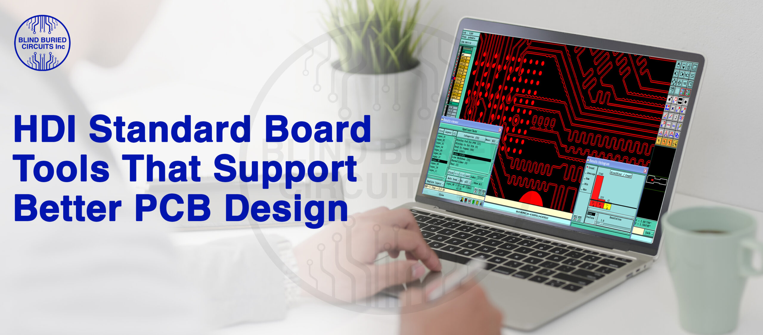
Modern HDI PCB success depends on using the right digital design tools that improve accuracy, signal integrity, manufacturability, and cost control.
Objective
To help you understand the key PCB design tools for HDI boards that support better layout decisions, stronger signal quality, and smoother production. You will also learn how these tools support manufacturability checks for HDI designs, so your board is easier to build the first time.
Key Takeaways
- HDI boards need better planning because there are few traces, vias, and parts.
- A strong tool set reduces design mistakes and saves time.
- A Stackup Designer helps you build reliable multilayer structures.
- An Impedance Calculator helps keep high-speed signals clean and stable.
- A Material Selector enables you to choose the right substrate for performance and heat control.
- Using these tools early improves DFM and reduces respins with any PCB manufacturer.

Table of Contents
- Introduction: Why HDI PCB Design Demands Advanced Tool Support
- The Role of Digital PCB Design Tools for HDI Boards in Modern HDI PCB Development
- Stackup Designer Tool for HDI Standard Boards
- Impedance Calculator Tool for HDI Standard Boards
- Material Selector Tool for HDI Standard Boards
- Combined Impact of HDI Board Tools on PCB Quality
- Best Practices for Using HDI PCB Design Tools Effectively
- Future Trends in HDI PCB Design Software and Automation
- Conclusion
- FAQs
Introduction: Why HDI PCB Design Demands Advanced Tool Support
HDI means High-Density Interconnect. In simple terms, it is a PCB design style that fits more connections into a smaller space. You do this using finer lines, narrower gaps, and specialised vias, such as microvias.
HDI PCBs are common in phones, wearables, medical devices, cameras, and many small electronics. These products need compact boards that still handle fast signals and power needs.
But HDI design is not easy. Parts like fine-pitch BGAs have pins packed very closely together. High-speed signals also react strongly to minor design changes. Even a tiny mistake in spacing or layer setup can cause noise, signal loss, or heat issues.
This is why innovative tools matter. Teams that work with Blind Buried Circuits often say that planning tools reduce risk in HDI projects because HDI boards have less room for trial and error.
In this blog, you will learn three essential HDI standard board tools:
- A Stackup Designer
- An Impedance Calculator
- A Material Selector
The Role of Digital PCB Design Tools for HDI Boards in Modern HDI PCB Development
Increasing density, speed, and miniaturization in electronics
Electronics keep getting smaller. But they also keep getting faster. This is a tricky mix.
When designs shrink:
- Trace widths go down
- Spacing becomes tighter
- Via sizes become smaller
- Layer counts often go up
At the same time, high-speed signals such as USB, DDR, PCIe, and RF require clean routing. They need controlled impedance and stable reference planes.
Risks of manual calculations and outdated workflows
Some teams still rely on:
- Hand calculations
- Old spreadsheets
- Generic online calculators
- Guess-and-check routing
This can cause:
- Wrong impedance targets
- Stackups that cannot be built
- Extra cost from unnecessary layers
- Routing that looks fine but fails in testing
A PCB board manufacturer can only build what is feasible. So if the design assumptions are wrong, you may face delays, changes, or rework.
Benefits of integrated HDI design utilities
When you use strong, modern tools, you get:
- Accuracy
- You avoid guesswork and reduce errors.
- Faster iteration
- You can test options quickly, such as trace-width changes or layer swaps.
- Reduced fabrication errors
- Tools help you catch issues before you send files out.
- Better cost optimization
- You can avoid adding layers that you do not need.
Stackup Designer Tool for PCB board manufacturer, Ready HDI Standard Boards
What an HDI PCB stackup includes
A stackup is the “layer plan” of your board. It defines what each layer does and the thickness of each material layer.
A typical HDI stackup includes:
- Signal layers (for routing traces)
- Plane layers (ground and power planes)
- Dielectric thickness between layers
- Copper weight per layer
- Spacing rules and build constraints
If the stackup is wrong, many other parts of the design become risky.
Key capabilities of an advanced stackup design tool
A strong Stackup Designer tool helps you with:
- Automated stackup generation
It can suggest layer structures based on goals, like impedance or layer count.
- Cost-optimized layer configurations
It enables you to compare options and avoid over-design.
- Built-in impedance planning
Many tools connect the stackup setup with impedance targets.
- Editable board parameters and real-time updates
When you change the dielectric thickness or the copper weight, the tool updates the values quickly.
Handling complex BGAs and controlled impedance requirements
HDI designs often include dense BGAs. You may need microvias, via-in-pad, and short escape routes. Stackup decisions affect how easily you can route these parts.
A Stackup Designer helps you plan:
- Layer count and routing capacity
- Ground reference layers for clean signals
- Via transition feasibility
- HDI build-up structures like 1+N+1, 2+N+2, and more
Practical benefits for PCB designers
When you use a Stackup Designer early, you get:
- Faster design validation
- You confirm the plan before the layout starts.
- Reduced re-spins
- You avoid stackup mistakes that cause rework.
- Improved collaboration with fabricators
- You send a clear plan to your PCB manufacturer, reducing DFM questions.
Impedance Calculator Tool for manufacturability checks for HDI designs
Why controlled impedance is critical in HDI layouts
Controlled impedance is about keeping the trace “electrical size” stable. High-speed signals behave like waves, not like simple DC lines.
If impedance is wrong, you may see:
- Reflections
- Signal ringing
- Data errors
- Higher EMI noise
This is common in fast interfaces. HDI boards often run these interfaces in tight spaces, so impedance control becomes even more important.
Core functions of a professional impedance calculator
A strong impedance tool supports:
- Accurate calculations
- Many tools use field-solver methods or advanced models.
- Support for microstrip and stripline
- Microstrip is on the outer layers. Stripline is inside the board.
- Single-ended and differential modeling
- Many signals use differential pairs, such as USB and PCIe.
- Unit flexibility and material references
- You can set material properties and units correctly.
This is why an impedance calculator is one of the most used PCB design tools for HDI boards.
Parameters designers can analyze
With a proper tool, you can analyze:
- Trace width and spacing
- Dielectric thickness
- Copper thickness
- Capacitance and inductance effects
- Propagation delay
- Effective dielectric constant
These details matter because HDI traces can be fragile and closely spaced.
Advantages over basic online calculators
Simple online calculators are helpful for learning. But they often miss real-world details.
A professional tool can be better because it considers:
- Real copper shapes and plating changes
- Actual dielectric behavior
- Better modeling for differential pairs
- Manufacturing tolerances that impact results
That also supports better manufacturability checks for HDI designs, because you can design with realistic build limits in mind.
Material Selector Tool for PCB design tools for HDI boards
Why dielectric material selection matters in HDI PCBs
Material is not just a “board base.” Material choices affect:
- Signal loss
- Heat handling
- Board stability over time
- Reliability in harsh conditions
If your material is not right, your board may warp, delaminate, or fail after repeated heating.
Features of an advanced PCB material comparison tool
A Material Selector tool often provides:
- A database of rigid and flexible materials
- Filters based on key properties
- Side-by-side comparison views
- Search by manufacturer or IPC style specs
This saves time and reduces the risk of wrong assumptions.
Key property categories that engineers evaluate
Electrical properties
- Dielectric constant (Dk)
- Dissipation factor (Df)
- Loss at high frequency
These affect signal speed and signal loss.
Thermal characteristics
- Glass transition temperature (Tg)
- Thermal conductivity
- Expansion rates
These affect heat handling and warpage.
Chemical resistance
- Resistance to moisture
- Resistance to chemicals used in cleaning or assembly
This matters for harsh environments and long-term reliability.
Mechanical strength
- Flex strength
- Peel strength
- Overall durability
This matters if the board faces vibration or bending.
How correct material selection improves manufacturability and cost
Better material decisions can:
- Prevent overheating and delamination
- Support high-frequency performance
- Reduce long-term failure risk
- Improve yield at your PCB board manufacturer
It also helps you avoid overpaying for a material you do not need.
Did You Know? HDI Facts
Did you know that microvias are often made with lasers and can be much smaller than traditional drilled vias? This helps designers connect layers in tight spaces, but it also makes process control more important for any PCB board manufacturer.
Combined Impact of HDI Board Design Tools on PCB Quality
Improved first-pass fabrication success
When stackup, impedance, and material choices align, the board is easier to build on the first try.
Reduction in redesign cycles and prototyping cost
Tools reduce the number of “surprise” issues during production and testing. That saves money and time.
Faster time-to-market for advanced electronics
When your design flows smoothly, you launch faster.
Better collaboration between designers and manufacturers
A design that includes clear notes, realistic constraints, and solid tool-based decisions makes it easier for the PCB board manufacturer to produce consistent results.
Best Practices for Using HDI PCB Design Tools Effectively
Validate stackup early in the design cycle.
Do stackup planning before heavy routing. This avoids big rework later.
Simulate impedance before routing completion
Check key nets early. Then confirm again before the final output.
Match material properties with signal speed and environment
High-frequency needs lower-loss material. High heat needs better thermal stability.
Coordinate with fabrication partners for DFM compliance.
Share early constraints with your PCB board manufacturer. Ask about:
- Minimum trace/space
- Microvia limits
- Via fill and plating rules
- Stackup build limits
Future Trends in HDI PCB Design Software and Automation
AI-assisted PCB stackup optimization
Tools may suggest better layer structures based on cost and impedance goals.
Real-time signal integrity simulation
More tools are moving toward instant checks during routing.
Cloud-based collaborative PCB design environments
Teams can work together faster, even across countries.
Integration with manufacturing data and digital twins
More tools will connect directly to real build data to improve accuracy.
Conclusion: Smarter Tools Lead to Better HDI PCB Performance
HDI design is robust but requires careful planning. The right tools reduce risk and improve quality.
A Stackup Designer helps you plan a strong structure. An Impedance Calculator enables you to protect high-speed signals. A Material Selector allows you to choose a substrate that meets your performance and heat requirements.
Together, these PCB design tools for HDI boards support better results and stronger manufacturability checks for HDI designs.
Teams that understand HDI well, like Blind Buried Circuits, know that good tools are not “extra.” They are a practical necessity when designing compact, high-performance boards.
If you want fewer delays with your PCB board manufacturer, start with better stackup, impedance, and material decisions early. It is one of the simplest ways to reduce rework and improve first-pass success.
FAQs
1) What are the best PCB design tools for HDI boards used by a PCB manufacturer’s team?
The best PCB design tools for HDI boards usually include a Stackup Designer, an Impedance Calculator, and a Material Selector. These help a PCB manufacturer-focused team make accurate stackup, impedance, and material decisions before production.
2) Why are manufacturability checks for HDI designs necessary before sending files to a PCB board manufacturer?
Manufacturability checks for HDI designs help confirm that trace spacing, via types, stackup thickness, and material choices can be built reliably. This reduces design changes and prevents delays when your PCB board manufacturer reviews the project.
3) How often should you use an impedance calculator in manufacturability checks for HDI designs?
You should use an impedance calculator early and again before the final output. The impedance targets must match realistic trace sizes and materials used by your PCB manufacturer.
4) What material properties matter most when selecting substrates for HDI boards?
Key properties include Dk, Df, Tg, and thermal expansion. These values affect signal loss and board stability. Material selection supports HDI design manufacturability checks, improving long-term reliability.


