Shrinking product sizes and rising power densities challenge engineers to build circuit boards that are both compact and robust. A critical step in achieving this reliability is proper PCB in via design and filling. Poorly handled vias can allow solder to wick through holes, create voids, or weaken mechanical strength leading to costly failures in the field.
This blog will help you to understand the key via filling techniques for PCB Fabrication, and explore widely available guidelines like IPC 4761 (for reference only), and share practical insights to help you produce long-lasting, high-performance boards.
Why PCB in Via Filling Matters for Modern Electronics
Vias are copper-plated holes that connect different layers of a printed circuit board. Each PCB in via is vital for electrical continuity and heat dissipation. If a via is not designed and filled correctly, signal integrity and mechanical stability can be compromised.
High-power applications must also account for the current capacity of via. Inadequate copper plating or fill can cause overheating and eventual failure. Whether you are designing a compact IoT module or an industrial power board, controlling via structure and fill is fundamental to long-term reliability.
Overview of Key Via Filling Methods and Materials
Selecting the right via filling approach depends on board density, component type, and cost targets. Below are the most common techniques applied during pcb in via fabrication.
Resin or Epoxy Processes for PCB in Via Filling
One proven technique is pcb in via filling with resin or epoxy. This method uses vacuum-assisted injection and thermal curing to create a solid plug inside each via. The result is a smooth surface that prevents solder migration during reflow, making it ideal for high-density interconnect (HDI) designs and boards requiring excellent surface planarity.

Types of Vias and When to Use Them
Designers can choose from several pcb via types including through-hole, blind, buried, and microvias. Blind and buried vias reduce layer count and save board space, while microvias support fine-pitch BGA components. The right combination of via types ensures both electrical performance and cost efficiency.

Capped or Plugged Via Options for High-Density Boards
In applications demanding an ultra-flat surface, a capped via where the filled hole is overplated with copper offers reliable solderability. Plugged vias, which are filled but not overplated, are suitable when component pads are not mounted directly on top.

Design Guidelines and Performance Considerations
Well-established standards and sound engineering calculations reduce risk and ensure predictable outcomes. Partnering with blindburiedcircuits means these guidelines are not just theory but actively applied in production, giving you designs that balance reliability, performance, and manufacturability.
Using IPC 4761 Principles as a Reference
Although we do not hold formal IPC 4761 certification, we align our practices with many of its core principles. IPC 4761 is an industry guideline describing methods for via protection and filling like tenting, plugging, and capping so that designers and fabricators share a common language. Referring to these concepts helps you communicate requirements clearly and avoid costly re-spins.
Ensuring Adequate Current Capacity of Via
Thermal buildup is one of the most common causes of via-related failure. Accurately calculating the current capacity of via based on copper thickness, fill material, and layer stackup make sure that every PCB in via can safely handle its expected load. Our engineering team incorporates these checks during the design review stage to enhance board longevity.
Practical Insights from PCB Manufacturing Experts
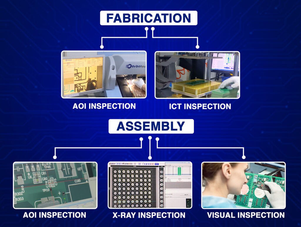
Production expertise often makes the difference between theory and flawless boards. A seasoned pcb manufacturing company offers precise drilling, controlled resin curing, and thorough X-ray inspection to detect voids or delamination early.
For example, in high-frequency telecom applications, we frequently recommend using conductive epoxy for selective pcb via filling, as it enhances thermal transfer. In power electronics, we may suggest using multiple parallel vias or thicker copper barrels to ensure the required current-carrying capability.
Common Mistakes
Even highly skilled design teams can sometimes miss important details that affect manufacturability and long-term performance:
- Voids or incomplete fills can allow solder to leak through vias, leading to shorts or reliability issues.
- Unbalanced copper distribution across layers increases the risk of board warpage during fabrication.
- Overlooking IPC 4761 recommendations for via treatment often results in unclear manufacturing instructions and unnecessary delays.
Email our experienced sales engineers at sales@blindburiedcircuits.com to help you to avoid these pitfalls, as we carefully review designs to ensure compliance with best practices and smooth handoff to production.
Conclusion: Building High-Reliability Boards with Better Via Filling
Whether it’s resin-based via filling or advanced capped-via techniques, selecting the right method helps achieve mechanical durability, electrical reliability, and efficient assembly. Even without formal IPC 4761 certification, applying its principles offers a solid framework for clearer communication and stronger, more reliable and robust designs.
Partnering with an experienced PCB manufacturing company will help you select the right via types, calculate safe current capacity of via, and maintain rigorous process control so every PCB in via supports long-term product success.
Contact our specialists today at sales@blindburiedcircuits.com or download our detailed guide to start designing with confidence.


