Objective
This guide explains how to choose high-speed PCB substrate materials for high-frequency signals. It helps USA readers understand what matters most in high-frequency PCB materials and how RF PCB material selection improves signal quality, heat control, and reliability. At Blind Buried Circuits, the right material choice can solve problems before a board is built.
Key Takeaways
- High-speed PCB substrate materials affect loss, stability, heat, and impedance.
- Good high-frequency PCB materials usually have low loss and stable electrical values.
- RF PCB material selection should match frequency, board stack-up, copper type, heat, and budget.
- Standard FR-4 can work for some designs, but not every RF job.
- Material data sheets should be checked carefully before production.
Why High-Speed PCB Substrate Materials Matter
When your PCB handles low-speed signals, material differences may not be obvious. But for high-frequency or RF applications, even small weaknesses in the substrate can cause:
- Signal loss over traces
- Unstable impedance
- Increased heat
- Timing shifts and signal distortion
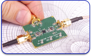
In high-speed boards, the substrate becomes part of the electrical system. Poor material choice can lead to tuning issues, test failures, and decreased product reliability, especially in:
- RF communication boards
- Radar systems
- Antenna circuits
- High-speed digital boards
- Satellite electronics
- Wireless devices
- Medical and test equipment
What Makes High-Frequency PCB Materials Different
Not all PCB materials are created equal. While standard laminates might work for basic digital circuits, high-frequency PCB materials are specifically designed for:
- Low electrical loss
- Stable signal speed
- Controlled impedance
- Heat resistance
- Moisture resistance
- Mechanical stability
These features ensure signals remain clean, repeatable, and accurate even at microwave and millimeter-wave frequencies.
Key Properties in RF PCB Material Selection
Selecting the right material starts with understanding the core properties that influence performance.
-
Dielectric Constant (Dk)
The Dk controls impedance, trace width, and signal timing. A stable Dk ensures predictable circuit behavior, which is essential in RF applications.
-
Dissipation Factor (Df)
Df measures how much signal energy the material absorbs. Lower Df reduces dielectric loss, keeping high-speed signals clean over long traces.
-
Thermal Stability
Materials must handle operating and assembly heat. Thermal instability can shift impedance and reduce board reliability.
-
Dimensional Stability
Stable materials maintain layer alignment and registration, avoiding performance shifts during fabrication and use.
-
Copper Surface Profile
Copper roughness affects conductor loss. Smooth surfaces reduce high-frequency signal attenuation, which is critical in RF designs.
| Property | What It Measures | Why It Matters in RF PCB Design |
| Dielectric Constant (Dk) | Impedance & trace width | Ensures predictable signal behavior |
| Dissipation Factor (Df) | Signal energy loss | Lower Df reduces dielectric loss |
| Thermal Stability | Heat tolerance | Maintains performance during operation & assembly |
| Dimensional Stability | Shape and layer alignment | Prevents misalignment and performance shifts |
| Copper Surface Profile | Copper roughness | Affects conductor loss and high-frequency signal quality |
Common High-Frequency PCB Material Families
-
Standard FR-4 and Enhanced FR-4
Suitable for lower RF ranges and mixed digital work, enhanced FR-4 materials (like I-Speed) offer improved loss performance compared to basic FR-4.
-
Hydrocarbon Ceramic Materials
Balancing RF performance and manufacturability, hydrocarbon ceramic laminates (such as Rogers RO4000 series) are ideal for microwave and millimeter-wave circuits.
-
PTFE-Based Materials
PTFE laminates (like Rogers RT/duroid) provide ultra-low dielectric constant and loss for demanding RF applications, though they require more careful processing.
| Material Type | Frequency Range | Advantages | Considerations |
| Standard/Enhanced FR-4 | <1–6 GHz | Affordable, easy to process | Higher Df, less stable at high frequency |
| Hydrocarbon Ceramic (e.g., Rogers RO4000) | 1–10 GHz | Low loss, stable Dk, good manufacturability | Slightly more expensive |
| PTFE-Based (e.g., Rogers RT/duroid) | >6 GHz | Ultra-low loss, excellent Dk stability | Difficult to process, higher cost |
Frequency Ranges Where Material Choice Becomes Critical
Material properties become more impactful as signal frequency rises. Generally:
| Frequency Range | Recommended Material |
| Below 1 GHz | Standard FR-4 |
| 1–6 GHz | Enhanced FR-4 / Hydrocarbon Ceramic |
| Above 6 GHz | PTFE-Based / High-Performance Ceramics |
Correct material choice ensures signal integrity, minimal insertion loss, and predictable impedance.
How Signal Loss Happens in High-Speed PCB Materials
Signal degradation in RF PCBs occurs due to:
- Dielectric Loss – Energy absorbed by the substrate
- Conductor Loss – Rough copper surfaces or thin traces
- Radiation Loss – Signals leaking from traces
- Impedance Mismatch – Changes in Dk or trace width
- Thermal Effects – Expansion or contraction affecting alignment
Understanding these mechanisms guides proper RF PCB material selection.
PCB Stack-Up Influence on RF Materials
Layer arrangement in a PCB (stack-up) affects impedance, crosstalk, and heat dissipation:
- High-speed signals need controlled spacing and consistent dielectric thickness
- Material choice must match the copper type and stack-up
- Incorrect combinations can lead to higher loss and signal distortion
Early planning prevents costly redesigns.
Step-by-Step RF PCB Material Selection Process
Follow this simple workflow:
- Define actual operating frequency and loss targets
- Check impedance and stack-up requirements
- Review thermal, environmental, and mechanical constraints
- Compare high-speed PCB substrate materials using Dk, Df, and stability
- Verify processing and fabrication compatibility
- Confirm availability and budget before production
A structured approach ensures reliable performance from the first build.
Mistakes To Avoid With High-Speed PCB Substrate Materials
- Choosing purely by the lowest cost
- Using material data at incorrect frequencies
- Ignoring copper roughness
- Overlooking thermal expansion and assembly stress
- Assuming all low-loss materials behave the same
- Mixing materials without checking the stack-up
Balanced material selection is the key to efficient and reliable RF PCB designs.
Conclusion
Choosing the right high-speed PCB substrate materials and making informed RF PCB material selection decisions is critical for high-frequency performance. By evaluating high-frequency PCB materials carefully and considering frequency, stack-up, thermal, and mechanical factors, designers ensure boards work reliably the first time. Blind Buried Circuits highlights that selecting the right materials is crucial for signal integrity, manufacturability, and long-term reliability.
FAQs
What Are The Best High-Speed PCB Substrate Materials For RF Work?
No single material fits every design. Choices depend on frequency, layers, loss targets, heat, and cost. Options include enhanced FR-4, hydrocarbon ceramic laminates, and PTFE-based laminates.
Can FR-4 Be Used in High-Frequency PCB Materials Projects?
Yes, for lower frequencies or less critical paths. Tighter RF designs often need lower-loss and more stable materials.
Why Is RF PCB Material Selection Important For Signal Quality?
Because the laminate directly affects signal loss, impedance, heat handling, and repeatability. Poor choice reduces performance and makes tuning difficult.
Does Lower Df Always Mean A Better Material?
Not always. Low Df reduces dielectric loss, but full selection considers Dk stability, thermal strength, manufacturability, and cost.


