Objective
This blog explains why the microvia aspect ratio matters in HDI board design and how manufacturers read that number before they accept a job. The goal is to help readers understand how aspect ratio affects drill depth, plating, build risk, and long-term reliability.
At Blind Buried Circuits, this matters because many HDI problems do not start during testing. They start much earlier, when a design asks a manufacturer to build a microvia structure that is too aggressive for stable production.
Key Takeaways
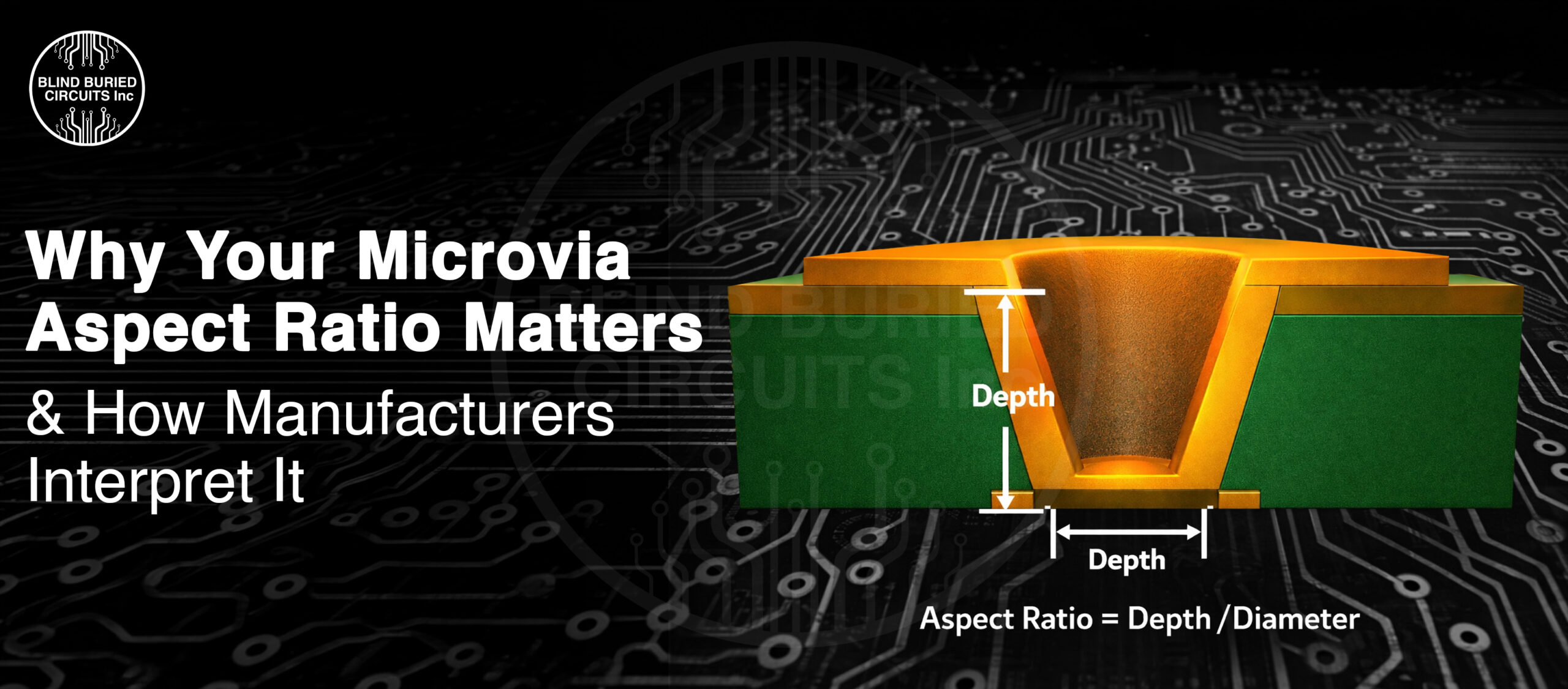
- The microvia aspect ratio compares microvia depth to microvia diameter.
- IPC and many manufacturers treat a microvia as a blind structure with a maximum aspect ratio of 1:1 and a total depth of no more than 0.25 mm.
- Many manufacturers prefer a safer target closer to 0.8:1 for better plating and reliability.
- A higher microvia aspect ratio can make laser drilling, copper plating, and copper filling harder.
- Good HDI PCB design guidelines start with real factory limits, not only what CAD software allows.
- Better aspect ratio choices improve microvia reliability in HDI PCBs.
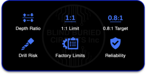
Table Of Contents
- What Microvia Aspect Ratio Means
- Why Manufacturers Care About Microvia Aspect Ratio
- How The Number Is Calculated
- What Manufacturers Usually Want To See
- How Laser Drilled Microvias Change The Picture
- Why Microvia Reliability In HDI PCBs Depends On Aspect Ratio
- How Manufacturers Interpret Your Design Files
- Common Design Mistakes That Raise Risk
- Practical HDI PCB Design Guidelines
- Conclusion
- FAQs
1. What Microvia Aspect Ratio Means
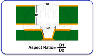
A microvia aspect ratio is the relationship between the depth of a microvia and its diameter. In simple words, it tells the manufacturer how deep the hole is compared with how wide it is. Altium explains microvia aspect ratio as outer-layer dielectric thickness plus outer copper foil thickness divided by microvia diameter. More generally, the aspect ratio is also commonly described as drill depth divided by drill diameter.
That number matters because a shallow and wide microvia is usually easier to process than a deep and narrow one. The deeper and narrower the hole gets, the harder it becomes to drill it cleanly and plate it evenly.
Did You Know? IPC-linked manufacturer guidance defines a microvia as a blind structure with a maximum aspect ratio of 1:1 and a total depth of no more than 0.25 mm.
2. Why Manufacturers Care About Microvia Aspect Ratio
Manufacturers do not look at the microvia aspect ratio as just a math value. They see it as a process risk signal. A high ratio may mean:
- Harder laser drilling
- More difficult desmear and cleaning
- Uneven copper plating
- More trouble with copper fill
- Higher defect risk
- Lower long-term reliability
That is why many shops do not simply ask, “Can it be drilled?” They ask, “Can it be drilled and plated well, every time, in production?” Guidance from NCAB and Epec both point in the same direction: staying closer to 0.8:1 to 1:1 helps manufacturability and reliability, while pushing beyond that raises risk.
3. How The Number Is Calculated
For a simple blind microvia, the calculation is usually based on the buildup thickness above the target layer and the finished microvia diameter. Altium states the formula as:
- Microvia aspect ratio = outer dielectric thickness plus outer copper foil thickness ÷ microvia diameter
That means copper thickness matters too. Designers sometimes focus only on the dielectric layer and forget that copper adds to the effective depth. This is one reason a manufacturer may push back on a design that looked acceptable at first glance.
A simple way to think about it:
- A smaller diameter raises the ratio
- Greater depth raises the ratio
- Thicker copper can also raise the ratio
4. What Manufacturers Usually Want To See
In many cases, manufacturers accept up to 1:1 for standard microvias. But many prefer something safer. The recommended ratio for a laser-drilled L1-L2 microvia is 0.8:1, while 1:1 is considered more advanced. NCAB also notes that the ideal typical ratio is around 0.8:1, with common microvia diameters around 80 to 100 microns.
This is important because “possible” is not the same as “comfortable.” A manufacturer may be able to build a 1:1 design, but they may still see it as less forgiving than a 0.8:1 design.
Did You Know? NCAB recommends 100-micron microvias for better reliability when copper filling is needed, and also suggests larger entry and capture pads where possible.
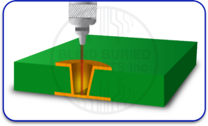
5. How Laser-Drilled Microvias Change The Picture
Most modern microvias are laser-drilled microvias. Laser drilling allows for smaller holes and tighter location control than mechanical drilling. Altium notes that typical hole sizes can be as small as 2 mil, and a typical maximum depth for a laser-drilled microvia is about 10 mil with a 1:1 aspect ratio. However, the exact numbers depend on the drilling system and the shop.
That sounds simple, but it changes how the manufacturer reads your files. They are not only checking drill size. They are checking:
- Laser drill capability
- Material type
- Copper thickness
- Layer buildup thickness
- Whether the microvia is filled
- Whether it is stacked or staggered
In other words, laser-drilled microvias create more routing freedom, but they still have real process limits.
6. Why Microvia Reliability In HDI PCBs Depends On Aspect Ratio
When people talk about microvia reliability in HDI PCBs, aspect ratio is one of the first things that matters. If the via is too deep for its diameter, plating can become uneven. The hole may be harder to clean. Filling can also become less consistent. Over time, those weak points can become failure points. Designers should maintain a 1:1 aspect ratio and avoid thick-copper situations that make reliable plating harder. It also notes that staggered microvias are generally preferred over stacked ones for better manufacturability and reliability.
That does not mean every 1:1 microvia is bad. It means the margin gets smaller as the ratio rises.
7. How Manufacturers Interpret Your Design Files
When a manufacturer opens an HDI package, they usually check more than the drawing notes. They look at the microvia structure in context.
They will often review:
- Layer-to-layer depth
- Finished hole size
- Capture pad size
- Copper weight
- Whether vias are stacked or staggered
- Fill requirements
- IPC class and inspection needs
This is where HDI PCB design guidelines become real. Microvias must be designed carefully to support routing between layers, and standard HDI stackups should be chosen early.
At Blind Buried Circuits, the key point is simple: manufacturers do not read a microvia note in isolation. They read the whole buildup and ask whether it can be built with a stable yield.
8. Common Design Mistakes That Raise Risk
Some microvia problems are caused by design choices that look small but create a lot of trouble later.
Common mistakes include:
- Pushing the microvia aspect ratio too close to the limit
- Using too small a diameter for the chosen buildup thickness
- Forgetting that copper thickness adds to effective depth
- Using stacked structures where staggered would be safer
- Asking for fill without enough process margin
- Making pads too small for reliable capture
NCAB guidance also warns that tighter geometries need direct consultation with the manufacturer.
9. Practical HDI PCB Design Guidelines
Good HDI PCB design guidelines around microvias are usually simple:
- Keep the aspect ratio conservative when possible
- Start with the largest workable microvia diameter
- Match the buildup thickness to the real shop capability
- Check the copper weight early
- Use staggered microvias when the design allows
- Review fill needs before final release
- Ask the fabricator for preferred rules, not just maximum rules
These steps help improve microvia reliability in HDI PCBs because they give the shop more room to drill, plate, and inspect the structure properly.
Conclusion
Your microvia aspect ratio matters because it tells the manufacturer how hard the via will be to build well. A design may still be possible at the edge of the limit, but a safer ratio often gives better yield, better plating, and better long-term performance. That is why manufacturers look closely at ratio, copper, depth, fill, and stackup before they commit to an HDI build. For Blind Buried Circuits, the smart approach is to design microvias for reliability first and density second.
Want fewer HDI surprises? Start with a fabricator review of microvia depth, diameter, stackup, and fill strategy before final release.
FAQs
What Is A Good Microvia Aspect Ratio?
Many manufacturers prefer a target near 0.8:1 for better reliability, while 1:1 is often treated as the upper practical limit for standard microvias.
Why Does Microvia Aspect Ratio Matter So Much?
It affects how easily the microvia can be laser drilled, cleaned, plated, and filled. Higher ratios usually mean higher manufacturing risk.
Are All Laser-Drilled Microvias Reliable?
Not automatically. Laser-drilled microvias can be very reliable, but the result depends on depth, diameter, material, copper thickness, and process control.
What Is The IPC Definition Of A Microvia?
IPC-linked manufacturer references describe a microvia as a blind structure with a maximum aspect ratio of 1:1 and a total depth of no more than 0.25 mm.
How Do Manufacturers Interpret Microvia Reliability In HDI PCBs?
They review the whole structure, including stackup, ratio, pads, fill, and whether the microvias are stacked or staggered. They want a build that can be repeated with a stable yield.
Should I Design To The Maximum Limit?
Usually no. Designing slightly inside the limit often gives better manufacturability and stronger long-term reliability.


