High-speed circuits in 2026 move a lot of data in very little time. That means timing margins are tight, and small layout choices can cause big problems. When a signal edge is fast, even a short trace can act like a transmission line. That is why you can see ringing, noise, and random errors when your routing and stackup are not well planned.
Traditional PCB designs can struggle here because vias are larger, trace spacing is wider, and routing paths are longer. Those limits can force messy layer changes and weak return paths. HDI helps by giving you fine lines, short paths, and better control near dense chips.
This blog will help you design for speed, stability, and manufacturability. It will also help you talk clearly with a pcb manufacturing company before you lock your design. If you follow work shared by Blind Buried Circuits, you have likely seen how small HDI choices can decide whether a high-speed board passes on the first build.
Objective
To help you design reliable high-speed HDI boards by focusing on stackup, routing, vias, power delivery, and manufacturing limits, with clear steps you can apply right away.
Key Takeaways
You will learn how to:
- plan a stackup that supports clean return paths and stable impedance
- improve signal integrity in HDI PCB design by reducing discontinuities
- handle microvia design in high-speed HDI PCBs without risking reliability
- reduce crosstalk, reflections, and noise in dense layouts
- design for test and manufacturing without painful redesigns

Table of Contents
- Understanding HDI PCBs in High-Speed Applications
- Stackup Planning for Signal Integrity
- Microvia Design and Reliability
- Controlled Impedance Routing in HDI
- Power Integrity and Decoupling Strategy
- Signal Integrity and Crosstalk Control
- EMI and EMC Considerations
- Component Placement for High-Speed HDI Boards
- Thermal and Mechanical Considerations
- DFM and Manufacturing Constraints
- Simulation, Validation, and Testing
- Common HDI Design Mistakes
- Conclusion
- FAQs
Did You Know?
Many high-speed problems do not come from the chip. They come from the path between chips. A small via stub, a split reference plane, or a poor decoupling loop can reduce eye opening even when your schematic is correct.
Understanding HDI PCBs in High-Speed Applications
What Defines an HDI PCB
An HDI PCB usually includes:
- microvias (often laser drilled)
- fine lines and tight spacing
- higher wiring density near dense ICs
- build-up layers added in stages
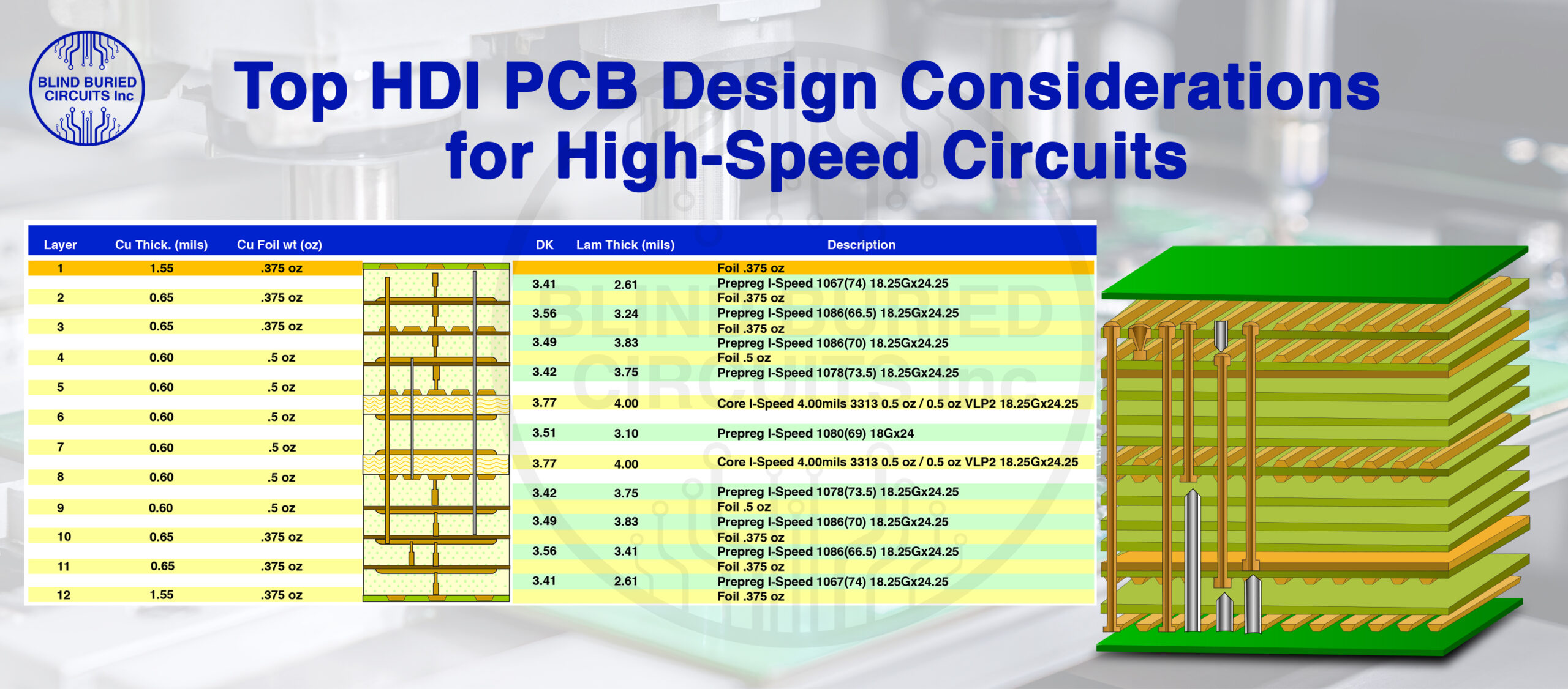
Common build-up structures include 1+N+1 and 2+N+2, where “N” is the core and the outer layers are added in steps.
Why High-Speed Circuits Demand HDI
High-speed designs benefit from HDI because you can route:
- shorter signal paths with fewer detours
- smaller via transitions with lower parasitics
- tighter power and ground structures close to the chip
This is the foundation of better signal integrity in HDI PCB design.
1) Stackup Planning for Signal Integrity in HDI PCB Design
Selecting the Right Number of Layers
More layers are not always better, but too few layers can force long routes and broken return paths. You want enough layers to keep:
- a nearby reference plane for every high-speed layer
- clean routing channels for key buses
- separate space for power distribution where needed
A simple rule: every fast signal layer should have a solid reference plane next to it.
Dielectric Material Selection
High-speed losses depend on the dielectric. In simple terms, lower-loss materials help signals stay cleaner over distance. If you are running long, high-speed lanes, ask your PCB manufacturer about low-loss options and consistency across build-up layers.
Focus on:
- stable dielectric thickness (helps impedance control)
- predictable material data for your simulation
- repeatability from lot to lot when possible
Reference Plane Continuity
Plane splits under high-speed traces are a common hidden problem. When the return path is broken, the current spreads out, and the noise rises.
Try to:
- avoid split planes under critical lines
- keep layer transitions near stitching vias
- maintain controlled impedance through the whole path

2) Microvia Design in High-Speed HDI PCBs and Reliability
Microvia Types and Use Cases
You will see:
- blind microvias (outer to inner)
- buried vias (inner to inner)
- stacked microvias (microvias on top of microvias)
- via-in-pad (via placed inside a component pad)
Via-in-pad is common for fine-pitch BGAs because it shortens the escape path and can improve signal integrity in HDI PCB design.
Aspect Ratio and Diameter Limits
Microvias have process limits. A good pcb manufacturing company will tell you the safe ranges for:
- microvia diameter
- capture pad size
- The dielectric thickness that the via must cross
If you push too hard, you risk cracks during thermal cycling. That matters for automotive, industrial, and other products that often require heating and cooling.
Via Transition Impact on Signal Quality
Every via transition can cause a small change in impedance. To reduce that:
- keep via depth as short as practical
- avoid extra layer changes on critical nets
- use stitching vias when changing reference planes
Back-drilling is often used to remove stubs from through vias. Microvias usually do not create large stubs, which is one reason microvia design in high-speed HDI PCBs is so helpful.

3) Controlled Impedance Routing in HDI
Trace Geometry and Line Width Control
Fine-line routing is robust but can be sensitive to variations. Copper thickness, etch bias, and dielectric thickness all influence impedance.
Practical steps:
- Use your PCB manufacturing company’s stackup data, not generic values
- set realistic rules for width and spacing
- Avoid last-minute stackup changes after routing is done
Differential Pair Routing Guidelines
Differential pairs need consistent geometry and length control. Keep:
- pair spacing stable through bends and neck-downs
- length mismatch within your timing budget
- layer changes are minimal, especially on long lanes
Managing Return Current Paths
Return current follows the lowest impedance path, usually right under the trace on a solid plane. Help it by:
- keeping a continuous ground plane under the route
- Adding stitching vias near layer transitions
- avoiding routing over gaps and voids
These steps directly support signal integrity in HDI PCB design.

4) Power Integrity and Decoupling Strategy
High-Speed Power Distribution Networks (PDN)
High-speed chips pull current in sharp bursts. If your PDN impedance is too high, you get voltage droop and noise. HDI helps because thin dielectrics can bring the planes closer together, reducing inductance.
Decoupling Capacitor Placement in HDI
Place key decouplers close to the pins they support. In many HDI layouts, via-in-pad for decouplers reduces loop area.
Good habits:
- shortest possible path from the cap to the power and ground
- multiple caps of different values for different frequency ranges
- clear return path to the ground plane
Plane Pairing and Embedded Capacitance
Closely spaced power and ground planes can add proper capacitance and reduce noise. This can help with simultaneous switching events, especially on wide buses.

5) Signal Integrity and Crosstalk Control
Reducing Near-End and Far-End Crosstalk
When traces are close, they couple energy. In HDI, spacing can be tight, so you must plan for it.
Use:
- spacing rules for critical nets
- ground shielding traces only when the return path stays clean
- ground vias to fence noisy areas when needed
Managing Reflection and Loss
Reflections result from impedance changes, such as stubs, neck-downs, and poor terminations. Loss comes from dielectric and copper effects.
Keep it practical:
- match impedance where it matters most
- avoid sudden width changes on long lanes
- Keep connectors and vias consistent across channels
6) EMI and EMC Considerations in High-Speed HDI Designs
High-speed edges create high-frequency energy. If you do not contain it, it can radiate.
Helpful controls:
- stitching vias near layer transitions
- ground fences along board edges for noisy sections
- short trace lengths where possible
- proper termination on fast lines
7) Component Placement for High-Speed HDI Boards
Placement Around High-Speed ICs
Start placement with the highest-speed parts first. Keep escape routing short and direct.
Fan-Out Strategies for Fine-Pitch Packages
For BGAs and CSPs, choose a fan-out style early. A dog bone can work for a larger pitch. Via-in-pad often works better for excellent pitch and supports a cleaner microvia design in high-speed HDI PCBs.
8) Thermal and Mechanical Considerations
Heat Dissipation in Dense HDI Designs
Dense routing can block copper areas that would otherwise spread heat. Balance signal needs with thermal paths using:
- thermal vias near hot parts
- solid copper where it does not harm routing
- careful plane cutouts that do not break return paths
Mechanical Reliability of Microvias
Microvias see stress during temperature changes. If your product cycles between hot and cold, avoid overusing stacked microvias without a clear reliability plan from your PCB manufacturer.
9) DFM and Manufacturing Constraints
HDI Fabrication Limitations
Every shop has limits on:
- minimum trace width and spacing
- microvia size and capture pad
- layer alignment tolerance
Early DFM Review for High-Speed HDI
Do not wait until you finish routing. Share your intent early and confirm:
- stackup and materials
- via structure
- impedance targets and test coupons
- inspection and reliability expectations
This is where talking with a PCB manufacturing company early saves you from redesign.
10) Simulation, Validation, and Testing
Pre-Layout and Post-Layout Simulation
Use simulation to check:
- timing margins and skew
- eye-opening and reflections
- PDN impedance trends
High-Speed Testing and Debugging
HDI boards have fewer easy test points. Plan probe access early. Use dedicated test pads on slower nets when possible, and consider connector breakouts for critical lanes during validation builds.
Common HDI Design Mistakes in High-Speed Circuits
These issues show up often:
- using stacked microvias everywhere without the need
- routing high-speed traces over split planes
- skipping stitching vias at reference changes
- placing decouplers far from the power pins
- trusting default material values instead of real stackup data
Conclusion
High-speed HDI design works best when you treat the board as a system. Stackup, vias, routing, power delivery, and manufacturing limits all interact. When you plan them together, you get cleaner signals, fewer surprises, and better first-pass success.
If you have followed technical work from Blind Buried Circuits, you already know that good HDI results come from small, disciplined choices made early. A strong partnership with a PCB manufacturing company also helps, because manufacturability is part of performance.
FAQs: HDI PCB Design for High-Speed Circuits
When should HDI be used for high-speed designs?
Use HDI when you have dense packages, tight routing channels, short timing margins, or when you need shorter vias and cleaner transitions to protect signal quality.
Are stacked microvias reliable for high-speed signals?
They can be reliable when designed within proven limits, built by a capable shop, and validated for the expected temperature cycling. They should be used only when they provide clear routing value, not as a default choice.
How many layers are ideal for HDI high-speed boards?
There is no single number. The best layer count depends on routing density, required return planes, and PDN needs. The goal is enough layers to keep return paths continuous and routing direct.
What data rates require HDI technology?
There is no hard cutoff because board size, trace length, and package density matter. HDI becomes more useful as edges get faster, traces get longer, and routing around fine-pitch devices becomes harder.


