Objective
This blog explains why PCB design complexity is rising so quickly in the U.S., and why many manufacturers are finding it hard to keep up. It looks at what is driving harder board designs, where factory limits show up, and what this means for engineers, buyers, and product teams. The goal is to make a technical topic easy to understand without losing accuracy.
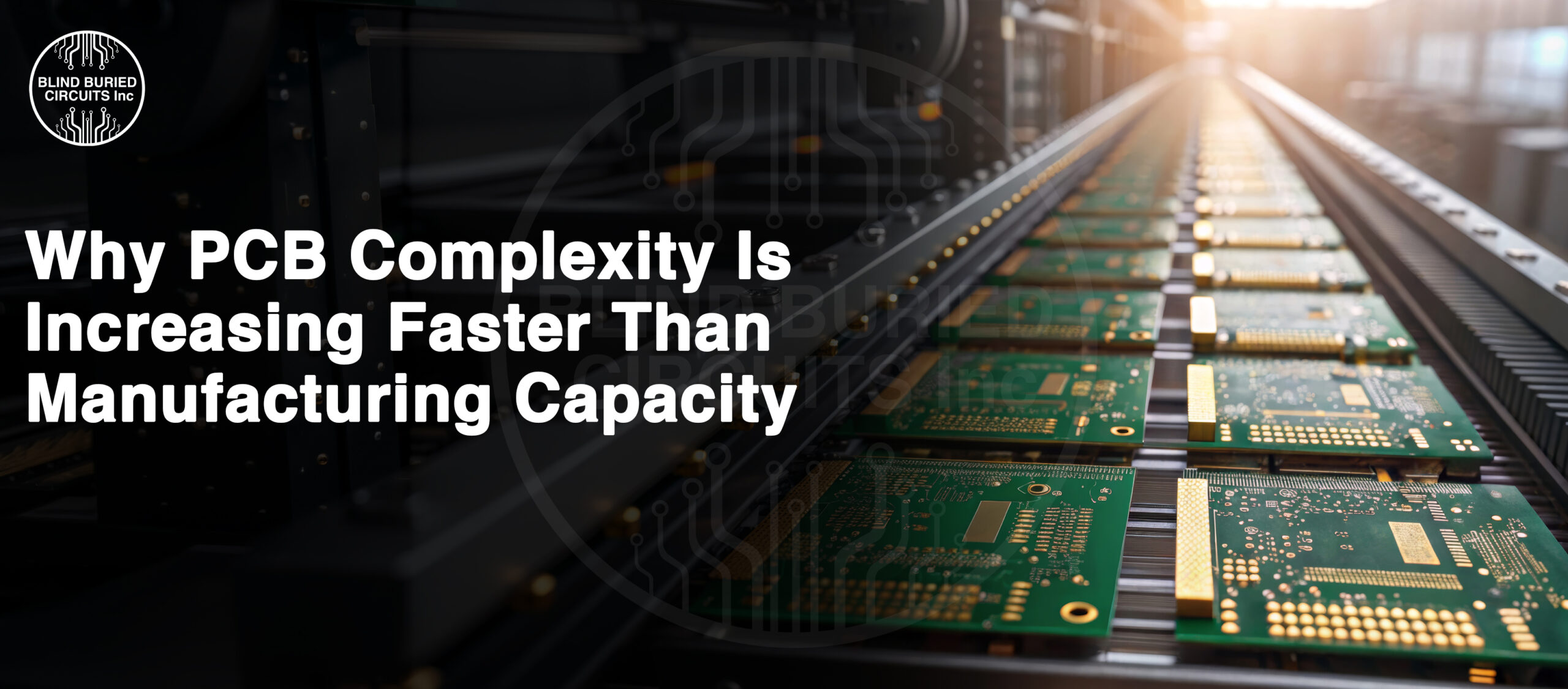
In simple terms, boards are being asked to do more than ever before. They must carry more signals, more power, and more functions in less space. That is why Blind Buried Circuits sees growing pressure on both design teams and fabricators as projects move from idea to production.
Key Takeaways
- PCB design complexity is rising because products are smaller, faster, and more feature-packed than before.
- Fine lines, microvias, stacked structures, and high layer counts are pushing factories closer to process limits.
- U.S. electronics demand is growing in advanced areas, but domestic capacity gaps still exist in PCBs, substrates, and advanced packaging.
- Many of today’s delays are caused by the gap between what designers can draw and what factories can build at scale.
- Better planning, earlier design reviews, and realistic fabrication choices can reduce risk.

Table Of Contents
- What PCB Design Complexity Means
- Why Boards Are Getting Harder To Build
- High-Density PCB Design Trends Are Raising The Bar
- Why Advanced PCB Manufacturing Challenges Are Growing
- The Real Limitations Of PCB Fabrication Processes
- Why Capacity Is Not Growing Fast Enough
- How This Problem Affects U.S. Product Teams
- What Engineers And Buyers Should Do Early
- Conclusion
- FAQs
1. What PCB Design Complexity Means
PCB design complexity means a board is harder to design, harder to build, or both. A simple board may have wider traces, fewer layers, larger parts, and easier drilling. A complex board usually has tighter spacing, more layers, smaller parts, more heat, and stricter signal rules. It may also need blind vias, buried vias, controlled impedance, or advanced stackups.
This matters because modern products are no longer simple. A single board may now support high-speed computing, wireless links, dense memory, sensors, thermal control, and tight mechanical limits all at once. That makes PCB design complexity a real manufacturing issue, not just a layout issue.
Did You Know?
Ultra-HDI work can involve line width and spacing below 50 microns, dielectric thickness below 50 microns, and microvia diameter below 75 microns. Those numbers show how fast design demands are shrinking.

2. Why Boards Are Getting Harder To Build
The biggest reason is simple: electronics keep getting smaller while performance keeps going up. Designers are asked to fit more into less space. That creates denser routing, more thermal stress, and tighter tolerances.
Several product trends are pushing this change:
- AI and data-heavy hardware
- Smaller medical and wearable devices
- Automotive electronics with more sensing and control
- Faster networking gear
- Compact industrial systems
As a result, PCB design complexity keeps rising even on projects that used to be considered normal. High-speed parts need cleaner routing. Dense BGAs need better fanout. Power-hungry products need stronger thermal paths. Mechanical teams also want thinner boards and smaller enclosures. All of that lands on the PCB.

3. High-Density PCB Design Trends Are Raising The Bar
One of the clearest causes of PCB design complexity is the move toward denser interconnects. Current high-density PCB design trends include finer lines, smaller vias, thinner dielectrics, and more advanced fanout methods. Semi-additive processes can repeatedly produce features around 15 microns, which opens new design options but also raises the skill and process level needed in fabrication.
Another major shift is Ultra HDI. Newer Ultra HDI fabrication can support trace widths and spacing as small as 25/25 microns, which helps route modern parts in tight spaces. That sounds great for design freedom, but it also means fewer factories can build the board reliably at volume.
These high-density PCB design trends are useful, but they create pressure in three ways:
- They need tighter process control
- They reduce the margin for error
- They increase cost and lead-time risk
This is where the design side and factory side start to pull apart. Designers can place smaller features in CAD faster than many plants can add new equipment, qualify new chemistry, and stabilize yields.
Did You Know? Double-sided BGA layouts can force much higher layer counts, especially when dense fanout and manufacturable via structures must work together.
4. Why Advanced PCB Manufacturing Challenges Are Growing
The phrase advanced PCB manufacturing challenges covers the gap between complex board requirements and real-world production limits. A board may look clean in software, but the factory must still image it, drill it, plate it, laminate it, register layers, and test it without defects.
The hardest advanced PCB manufacturing challenges often include:
- Fine line etching control
- Microvia formation and filling
- Layer-to-layer registration
- Thin dielectric handling
- Yield loss on dense designs
- Thermal warpage during build
- Inspection difficulty on small features
These challenges are not small details. Every tighter feature raises the chance of scrap, rework, or lower yield. That is one reason manufacturing capacity does not rise as fast as design ambition. It is not enough to buy a machine. A factory also needs process knowledge, qualified operators, stable materials, and repeatable output.
5. The Real Limitations Of PCB Fabrication Processes
A lot of teams learn this lesson late: design rules are not the same as process reality. The limitations of PCB fabrication processes show up when a board pushes too many hard features at the same time.
Common limitations of PCB fabrication processes include:
- Minimum trace and space limits
- Drill aspect ratio limits
- Registration tolerance limits
- Plating consistency limits
- Material handling limits
- Test access limits
For example, if a design uses ultra-fine features, stacked microvias, thin materials, and high layer counts together, each added feature makes the process window smaller. A board may still be possible, but not every shop can build it well, and not every shop can build it in a useful volume.
That is why PCB design complexity keeps outrunning the shop floor. Design tools keep improving. Feature demands keep shrinking. But fabrication remains a physical process with yield limits, tool limits, and material limits.
6. Why Capacity Is Not Growing Fast Enough
The capacity side has its own problem. U.S. industry groups and policy filings continue to point to capability gaps in PCBs, substrates, and advanced packaging. IPC told the U.S. government in 2025 that IC substrate and PCB manufacturing are among the most vulnerable segments and that the United States lacks meaningful capability or capacity in several advanced electronics areas.
This matters because more board demand is moving toward complex builds, not simpler ones. Even when a new investment appears, it often takes years to install equipment, validate processes, train staff, and move customers into steady production. Capacity does not grow overnight.
There is also a second issue. Some of the hardest boards now sit close to advanced packaging and substrate territory. That creates overlap between PCB manufacturing, substrate work, and packaging infrastructure. North America has long faced gaps in that broader ecosystem.
So the problem is not just “not enough factories.” There are “not enough qualified factories for the hardest boards.”
7. How This Problem Affects U.S. Product Teams
For U.S. teams, the effect shows up in practical ways:
- Longer quoting cycles
- More DFM feedback
- Higher prototype costs
- Fewer supplier options
- Greater yield risk
- More redesign loops
- More sourcing pressure on parts and materials
This also changes how engineers should think about project timing. A board that looks advanced and efficient in layout may become slow and expensive if it exceeds normal manufacturing capability. BOM and supply chain visibility also now matter more because design risk and sourcing risk are tied together. Modern BOM tools are being used to track lead times, supplier risk, and compliance earlier in the design flow.
8. What Engineers And Buyers Should Do Early
The best response is not to avoid advanced boards. It is to plan more honestly.
Here are the steps that help most:
- Review stackup early
- Confirm real factory capability before release
- Ask about line, space, via, and yield limits
- Reduce unnecessary layer count when possible
- Avoid using the hardest features everywhere
- Align design, sourcing, and manufacturing teams sooner
- Treat DFM as part of design, not a late check
Connected manufacturing is also becoming more important. Industry discussions in 2025 highlighted how better data flow from design into machines can reduce mistakes and improve output.
Did You Know? Newer PCB workflows now connect design data, BOM intelligence, compliance checks, and supplier visibility more closely than before, which helps teams catch risk earlier.
Conclusion
The reason PCB design complexity is increasing faster than manufacturing capacity is simple in theory, even if hard in practice. Product demands are moving faster than factory expansion. Designers can ask for smaller features, denser routing, and more advanced structures right now. But manufacturers need time, capital, process control, and trained people to build those boards reliably and at scale.
Better results come from early design review, realistic process choices, and a clear understanding of the advanced PCB manufacturing challenges and limitations of PCB fabrication processes before release. That is how Blind Buried Circuits help bridge the gap between what is possible in software and what is reliable in production.
Want fewer surprises on a complex board? Start with a design review that checks density, stackup, vias, yield risk, and supplier fit before fabrication begins.
FAQs
What Is PCB Design Complexity?
PCB design complexity means a board has tighter features, more layers, stricter electrical needs, smaller parts, or harder manufacturing demands than a standard board.
Why Is PCB Design Complexity Rising So Fast?
It is rising because electronics need more power, speed, and function in smaller spaces. That pushes designers toward denser layouts and more advanced structures.
What Are The Biggest Advanced PCB Manufacturing Challenges?
Key advanced PCB manufacturing challenges include fine line control, microvias, layer registration, plating quality, thin materials, and yield management on dense boards.
What Are The Main Limitations Of PCB Fabrication Processes?
The main limitations of PCB fabrication processes include minimum trace width, spacing, drill limits, registration limits, plating limits, and the ability to build small features with good yield.
Why Is Manufacturing Capacity Lagging Behind?
Capacity lags because building advanced capability takes time, money, skilled labor, process control, and broader ecosystem support. U.S. industry filings also point to ongoing gaps in PCB, substrate, and packaging capability.
How Can Teams Reduce Risk On Complex PCB Projects?
They can reduce risk by reviewing stackup early, confirming supplier capability, using DFM sooner, and matching design choices to real process limits before release.


