Standard FR4 has been the default PCB material for decades. It is cheap, widely available, and works well for most applications.
But “most applications” are changing fast.
Today’s electronics run hotter, faster, and in harsher environments than FR4 was originally designed to withstand. When a board needs to carry 77 GHz radar signals, withstand engine-bay temperatures, and fit inside a space smaller than a matchbox, FR4 starts to fail. Not dramatically. Quietly. Signals degrade. Heat builds up. Reliability drops.
That is the problem Blind Buried Circuits sees engineers run into repeatedly. And that is exactly the problem hybrid PCBs were built to solve.
Key Takeaways
- A hybrid PCB combines two or more different substrate materials in one board construction, with each material selected for the specific role of that layer.
- The core drivers of hybrid PCB growth in 2026 are rising operating frequencies, higher thermal loads, and the cost barrier of all-premium-laminate construction.
- The hybrid PCB manufacturing process requires multi-cycle lamination, material-specific surface preparation, optimized drilling for mixed-hardness stacks, and controlled impedance verification. It is significantly more complex than standard fabrication.
- Key benefits of hybrid PCB design include better RF signal performance, improved thermal management, rigid-flex packaging options, cost efficiency on high-performance designs, and reliability in harsh environments.
- Multilayer hybrid PCBs are now a production standard in 5G, automotive radar, aerospace, medical imaging, and high-speed computing.
- Hybrid PCB capability varies widely between fabs. Qualifying your manufacturer’s PTFE surface preparation, using reliability data, and hybrid-specific process controls is essential before placing production orders.
What Is a Hybrid PCB
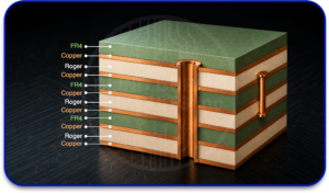
A hybrid PCB is a printed circuit board built from two or more different substrate materials stacked together in a single construction.
Think of it this way. A standard multilayer board uses the same material on every layer, FR4 from top to bottom. A hybrid PCB deliberately breaks that rule. It uses a high-performance laminate on the layers that need it and standard FR4 on the layers that do not.
The most common combination is FR4 paired with a low-loss RF laminate, such as Rogers 4350B, or a PTFE-based material. But hybrid PCBs also combine rigid layers with flexible polyimide layers, standard laminates with metal-core layers for thermal management, and ceramic-filled materials with conventional substrates for high-temperature applications.
The principle behind all of these is the same. Use the right material in the right place. Nothing more, nothing less.
This matters because premium laminates are expensive. Rogers 4350B costs roughly 10 to 20 times as much per square foot as standard FR4. Building a 10-layer board entirely from Rogers when only two layers actually carry RF signals is wasteful. Hybrid construction solves that directly, you get the performance where you need it without paying for it everywhere you do not.
Why 2026 Is a Turning Point for Hybrid PCB Adoption
Hybrid PCBs are not new. Engineers have been building them for years in aerospace and defense applications. What is new is the extent to which the need for them has spread.
Three things are driving this.
Frequencies are going up across consumer and industrial markets. 5G mmWave infrastructure operates between 24GHz and 100GHz. Automotive radar for ADAS systems runs at 76GHz to 81GHz. These are no longer niche military applications; they are in cars, smartphones, and warehouses. At these frequencies, standard FR4 becomes a problem. Its dielectric constant sits between 4.2 and 4.8 and varies with temperature and frequency. Its dissipation factor is around 0.02. Both numbers cause signal loss that cannot be tolerated at high frequencies. Rogers 4350B, by comparison, has a dielectric constant of 3.48 that stays stable, and a dissipation factor of 0.0037. That difference is not marginal; it is the gap between a working system and one that does not meet spec.
Thermal loads are higher than ever. Power electronics, EV battery management systems, and high-density computing boards generate heat that standard FR4 cannot conduct away. FR4 has a thermal conductivity of approximately 0.3 W/m·K. Metal-core hybrid substrates have a thermal conductivity of 2 to 8 W/m·K. For boards where heat is a reliability concern, that range is critical.
All-premium laminate is not financially practical at scale. Even when an engineer knows they need a better material, building an entire board from premium laminate is often not cost-effective. Hybrid construction is the practical middle ground: use what the design actually needs, layer by layer.
How the Hybrid PCB Manufacturing Process Works
The hybrid PCB manufacturing process is genuinely more complex than standard PCB fabrication. It is worth understanding why, because it directly affects how you design and which fab you choose.
Stack-Up Design Comes First
Before anything is manufactured, the stack-up must be precisely defined. This means deciding which layers use which material and how those layers bond together.
For a typical RF hybrid board, high-frequency laminate layers sit where RF and microwave signals route. FR4 layers carry digital signals, power planes, and ground references. The goal is to isolate each material to the role it performs best.
The biggest challenge at this stage is CTE (coefficient of thermal expansion). FR4 and PTFE-based laminates expand at different rates when heated. At vias that pass through both material types, this mismatch creates mechanical stress under thermal cycling. If the stack-up is not carefully accounted for, barrel cracking shows up in the field months after production. This is one of the most common failure modes in poorly designed hybrid PCBs.
Lamination Is More Involved
A standard multilayer PCB goes through one lamination cycle. Hybrid PCBs often need multiple cycles because different materials require different bonding temperatures and pressures.
PTFE-based laminates need surface preparation before they will bond reliably. PTFE is naturally non-adhesive, so the surface must be chemically etched, typically using sodium naphthalene treatment or plasma activation, before the adhesive layer is applied. Fabs that skip or rush this step produce boards that look fine initially but delaminate under thermal stress.
The bonding film between dissimilar layers also needs careful selection. A bonding film that introduces dielectric variation at the material interface will degrade controlled-impedance performance on RF layers, sometimes enough to push the design out of spec.
Drilling Requires Different Parameters
Drilling through a hybrid stack is harder than drilling through a uniform material. PTFE is soft and tends to smear at the drill hole wall, hindering copper plating adhesion inside the via barrel. Ceramic-filled laminates are abrasive and wear tooling faster than FR4.
A fab with genuine hybrid PCB manufacturing experience optimizes drill speed, feed rate, and tool life specifically for the hybrid stack, not for any single material within it. This sounds like a process detail. In practice, it determines whether your vias are reliable.
Testing Is More Extensive
Multilayer hybrid PCBs typically use ENIG or ENEPIG surface finish. HASL is usually avoided because the thermal shock of hot-air leveling puts stress on the bonds between dissimilar laminates.
Electrical testing covers opens and shorts as standard. Controlled-impedance testing of RF layers is essential, verifying that traces meet their target impedance values, typically 50 ohms for RF signal lines. Any deviation outside tolerance on a high-frequency layer causes reflection and signal loss that simulation would not have predicted.
The Real Benefits of Hybrid PCB Design
The benefits of hybrid PCB construction are specific. They solve real problems that single-material boards cannot.
Signal integrity at high frequencies. The lower dielectric constant and dissipation factor of RF laminates directly reduce insertion loss on high-frequency signal layers. At 10GHz, signal loss on FR4 is typically 3 to 5 times higher than on Rogers 4350B over the same trace length. For radar, 5G, and satellite systems, that difference determines whether the link budget closes.
Thermal performance. Hybrid constructions that incorporate metal-core layers, aluminum or copper, provide a direct path for heat to escape from the board. This extends component life in power electronics and LED driver applications where sustained operating temperature is the primary reliability driver.
Weight and space savings through rigid-flex construction. Hybrid rigid-flex boards eliminate the need for connectors and cable harnesses between PCB assemblies. In aerospace and medical devices, this reduces weight, improves vibration tolerance, and enables packaging geometries that cannot be achieved with rigid boards.
Cost efficiency on performance-critical designs. Using premium laminate only on the layers that need it, rather than the entire board, brings the cost of a high-performance design into a range that is actually manufacturable at scale. This is one of the most practical benefits of hybrid PCB design for commercial product development.
Harsh environment reliability. Ceramic-filled hybrid laminates operate reliably at temperatures above 250°C. FR4 starts to degrade above 130°C, depending on grade, up to 170 °C. For oil and gas downhole tools, aerospace avionics, and industrial equipment operating in extreme conditions, this thermal stability is not optional.
Hybrid PCB Vs Standard FR4 PCB: Comparison Table
| Comparison Point | Hybrid PCB | Standard FR4 PCB |
| Basic Meaning | Uses more than one material type in the same board stack-up. | Uses FR4 glass-reinforced epoxy material throughout the board. |
| Main Purpose | Used for designs that need high-speed signals, RF performance, thermal control, or power handling. | Used for general electronic circuits with standard performance needs. |
| Material Type | Combines FR4 with materials such as Rogers, PTFE, ceramic-filled laminates, metal core, or other specialty laminates. | Uses standard FR4 laminate and prepreg. |
| Signal Performance | Better for RF, microwave, and high-speed digital signals. | Suitable for low to medium-speed circuits. Signal loss increases at higher frequencies. |
| Thermal Performance | Can manage heat better when designed with high-performance or metal-backed materials. | Offers moderate thermal performance. Extra heat control may be needed for high-power boards. |
| Cost | More expensive due to specialty materials and complex fabrication. | More cost-effective and widely available. |
| Manufacturing Complexity | More complex because different materials behave differently during lamination, drilling, and plating. | Easier to manufacture because FR4 is standard and widely supported. |
| Lead Time | Usually longer due to material sourcing and fabrication control. | Usually shorter because FR4 is commonly stocked. |
| Common Applications | RF boards, antennas, aerospace electronics, radar systems, communication boards, and advanced test systems. | Consumer electronics, industrial controls, IoT devices, LED boards, and general embedded systems. |
| Best Use Case | Best when one PCB must support mixed RF, high-speed, thermal, or power requirements. | Best for standard, cost-sensitive designs that do not need specialty material performance. |
Where Hybrid PCBs Are Used Today
The applications pushing hybrid PCB adoption in 2026 are not hard to identify. They are wherever standard materials have hit their limits.
5G infrastructure uses hybrid boards combining low-loss RF laminates on antenna signal layers with FR4 for digital control and mechanical structure. Massive MIMO arrays and mmWave beamforming modules are almost impossible to build to spec on all-FR4 construction.
Automotive radar sensors operating at 77GHz require laminates with stable dielectric properties across the full automotive temperature range, from cold starts at -40°C to sustained engine-bay heat above 125°C. FR4 cannot maintain consistent impedance across that range.
Aerospace and defense systems, phased array radar, electronic warfare, and satellite communications use multilayer hybrid PCBs that combine RF laminates, controlled-impedance routing, and metal-core thermal management in a single integrated board.
Medical imaging equipment, including ultrasound probes and CT detector assemblies, requires RF signal performance and dimensional stability across repeated sterilization cycles.
High-speed computing backplanes running SerDes interfaces at 56Gbps and above benefit from low-loss laminates on critical signal layers, keeping cost-effective FR4 on power distribution and lower-speed routing layers.
At Blind Buried Circuits, we work with teams across all of these sectors. The pattern is consistent; engineers reach for hybrid PCB construction when a single material no longer meets the design’s requirements.
FAQs
Q1. What is the most common material combination used in a hybrid PCB, and why?
Rogers 4350B paired with FR4 is the most widely used combination. Rogers 4350B has a stable dielectric constant of 3.48 and a dissipation factor of 0.0037, both significantly better than FR4 for high-frequency signal routing. FR4 handles power distribution, ground planes, and digital signal layers at standard cost. This pairing gives RF and microwave designs the signal performance they need without the cost of building the entire board from premium laminate.
Q2. How serious is the CTE mismatch problem between FR4 and PTFE-based laminates?
It is a real reliability risk if not managed properly. FR4 has a CTE of approximately 14 to 17 ppm/°C in the x-y plane. PTFE-based laminates typically run 17 to 24 ppm/°C. At vias passing through both materials, this differential causes mechanical stress during thermal cycling. Over hundreds of cycles, it can crack via barrels or lift pads. Managing it requires minimizing through-vias at material interfaces, using filled and capped vias where connections must pass through the interface, and selecting compatible bonding films that absorb differential movement.
Q3. How is a hybrid PCB different from a standard multilayer PCB?
A standard multilayer PCB uses the same base material, typically FR4, on every layer throughout the stack. A hybrid PCB uses two or more different materials on different layers within the same stack. The fabrication process is more complex: lamination occurs in multiple cycles, and drilling parameters must account for the different mechanical properties of each material. The result is a board that delivers layer-specific performance that no single
material can match on its own.
Q4. What questions should I ask a fab to confirm they can build hybrid PCBs correctly?
Ask three things specifically. First, which hybrid material combinations have you qualified and run in actual production, not just evaluated? Second, how do you prepare PTFE surfaces before lamination, and is that step done in-house? Third, what via reliability data do you have from thermal cycling tests on hybrid stacks? A fab that answers all three with specific data has genuine capability. A fab that gives general answers about “experience with advanced materials” probably does not.
Q5. At what frequency does it make sense to switch from all-FR4 to a hybrid PCB approach?
As a practical guideline, designs with signal frequencies above 1 GHz should consider hybrid construction. The insertion-loss advantage of low-loss laminates becomes meaningful around 1 GHz and increases significantly with frequency. Above 5GHz, FR4 loss on most trace lengths will exceed the link budget for sensitive RF systems. Above 10GHz, all-FR4 construction is rarely viable for anything other than very short trace lengths. Calculate insertion loss for your specific trace lengths and frequencies on both materials; that calculation tells you where FR4 stops being adequate for your design.
Q6. Can hybrid PCBs be used for high-volume production, or are they only practical for low-volume and aerospace applications?
Hybrid PCBs are in high-volume production today. Automotive radar sensors, 5G base station antenna modules, and consumer mmWave devices all use hybrid PCB construction at production volumes of thousands to millions of units. The key is working with a fab that has validated hybrid processes at production scale, not just prototype capability. The cost per unit declines significantly at higher volumes as process yield improves and material purchasing scales.


