

Objective
To explain the difference between SMD components and SMT technology, how they work together, and the key factors affecting PCB assembly quality and reliability.
Key Takeaways
- SMD (Surface Mount Device) is the physical component mounted on a PCB. SMT (Surface Mount Technology) is the process used to mount it. They’re related, not interchangeable.
- Common SMD components include resistors, capacitors, diodes, transistors, ICs, LEDs, sensors, and connectors in package formats ranging from passive chip sizes (0201, 0402, 0603) to fine-pitch ICs (QFN, BGA, QFP).
- A standard SMT assembly line runs: solder paste printing → pick-and-place → reflow soldering → inspection → testing.
- Package type, pad pitch, and thermal mass all affect which reflow profile and inspection method a board needs.
- Choosing an SMT assembly partner depends on component package capability, PCB manufacturability, sourcing, and inspection requirements, not just whether they “do SMT.”
Table Of Contents
- Introduction
- What Are SMD Components?
- What Is SMT in Electronics?
- SMD vs. SMT: Key Differences
- How SMD Components and SMT Work Together
- Key Features of SMD Components
- Key Features of SMT Technology
- Factors to Consider When Choosing SMT PCB Assembly
- Common Applications of SMT Circuit Boards
- Why Choose Blind Buried Circuits for Your PCB Projects?
- Frequently Asked Questions
Introduction
SMD and SMT are closely related terms in PCB assembly, but they describe different things. SMD (Surface Mount Device) refers to an electronic component designed for surface mounting, while SMT (Surface Mount Technology) refers to the assembly technology used to place and solder those components onto a PCB. In simple terms, SMD is the component; SMT is the process.
Understanding the difference becomes important during PCB design and manufacturing because SMD package selection affects more than component size. Package geometry can influence the PCB land pattern, stencil aperture design, solder paste deposition, placement requirements, reflow behaviour, inspection and rework.
This guide explains the difference between SMD and SMT, how they work together in PCB assembly, and the manufacturing factors engineers should consider when selecting surface-mount packages and an SMT assembly process.
What Are SMD Components?
An SMD is an electronic component designed to sit directly on the copper pads of a PCB surface, soldered in place with no drilled through-holes, no leads passing through the board.
Common SMD components include:
- Resistors and capacitors (chip packages like 0201, 0402, 0603, 0805)
- Diodes and transistors (SOT-23, SOD-123)
- Integrated circuits (QFN, QFP, SOIC, BGA)
- LEDs
- Sensors and connectors
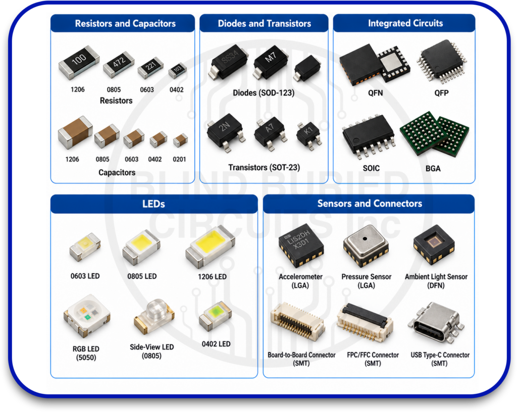
Package size drives a lot of downstream decisions. A 0201 resistor saves board space but is harder to place, inspect, and rework than an 0805. A fine-pitch QFN or BGA needs tighter solder paste control and, often, X-ray inspection to confirm joints hidden under the package. For an SMD prototype board, it’s worth choosing packages your assembler can place reliably at low volume, not just the smallest footprint on the datasheet.
SMD components show up across consumer electronics, industrial equipment, automotive systems, medical devices, communications gear, IoT devices, and aerospace/defense electronics anywhere on board space and component density matter.
What Is SMT in Electronics?
SMT is the assembly technology used to attach SMD components to PCB pads. A typical SMT process looks like this:
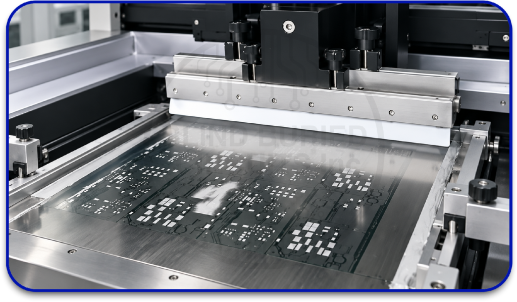
- Solder paste printing – paste is applied through a stencil onto the pads.
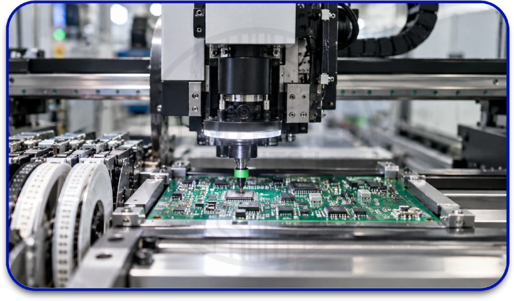
 2. Component placement – a pick-and-place machine positions each SMD.
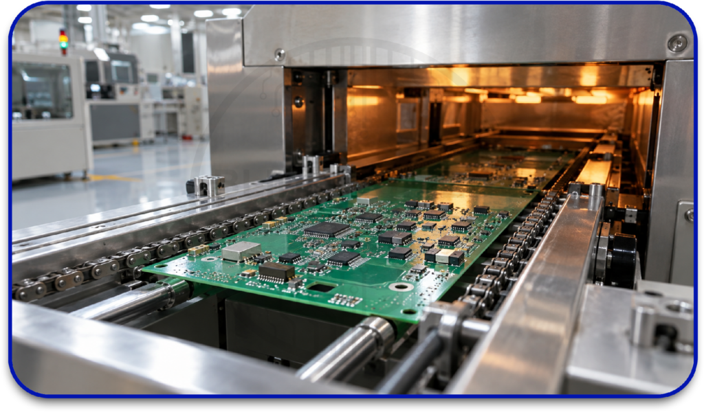
3. Reflow soldering – the board passes through a heated oven that melts the paste and forms solder joints. Profile temperature and dwell time are tuned to the paste alloy and the board’s thermal mass – get this wrong and you risk tombstoning small passives or incomplete joints on large ICs.
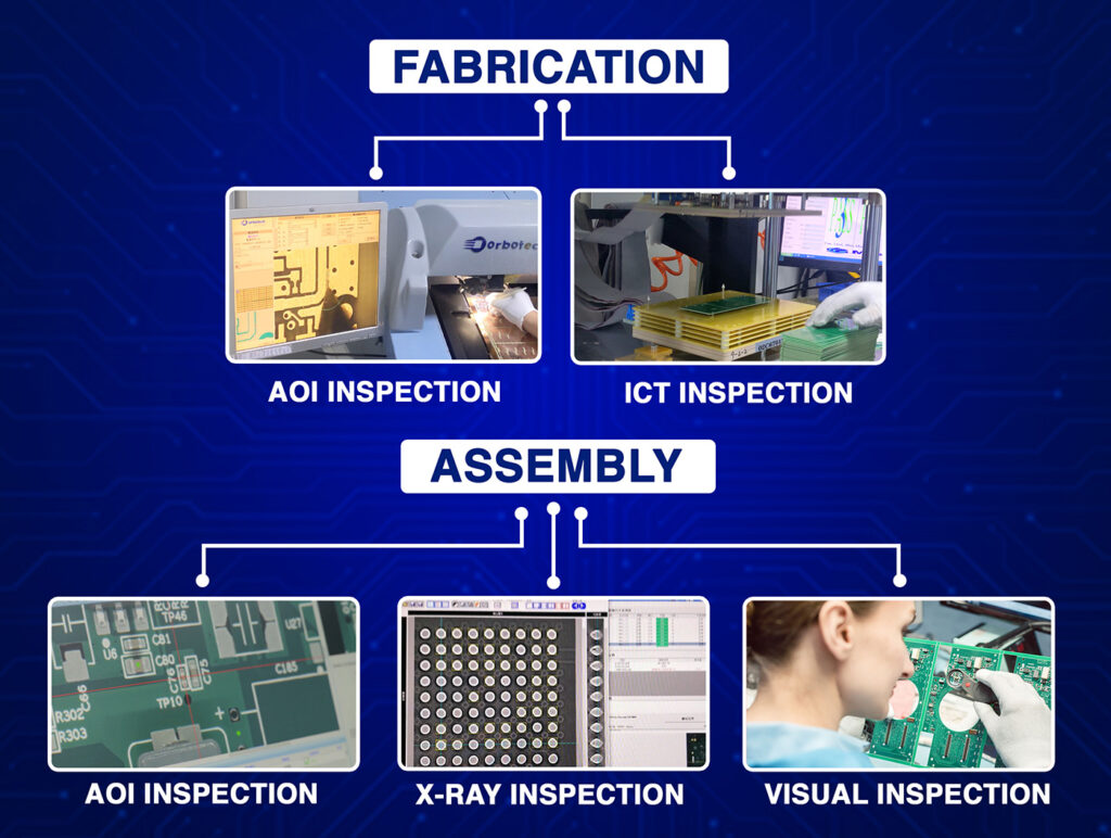
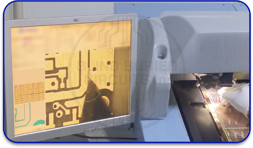
4. Inspection – automated optical inspection (AOI) checks visible joints; X-ray inspection checks hidden joints under BGAs and QFNs.
5. Testing – electrical or functional testing, depending on the product.
Modern SMT lines lean on automated placement and closed-loop process control, especially for dense boards or higher-volume runs where manual placement isn’t practical or repeatable.
SMD vs. SMT: Key Differences
| Feature | SMD | SMT |
|---|---|---|
| Full form | Surface Mount Device | Surface Mount Technology |
| Refers to | The physical component | The assembly process |
| Purpose | Provides an electrical function | Mounts and solders components to the board |
| Examples | Resistor, capacitor, IC, diode, LED | Solder paste printing, placement, reflow |
| Relationship | Used in SMT assembly | Used to assemble SMD components |
How SMD Components and SMT Work Together
- Solder paste application – a stencil deposits paste onto the pads that need a component.
- Component placement – the pick-and-place machine sets each SMD onto its paste-covered pads, guided by the pick-and-place program built from the PCB’s centroid/placement data.
- Reflow soldering – the board moves through a multi-zone oven (preheat, soak, reflow, cooling) that forms the solder joints.
- Inspection – AOI catches visible defects like tombstoning, bridging, or missing components; X-ray inspection checks joints hidden under packages like BGAs.
- Testing – in-circuit or functional testing confirms the board performs as designed.
Key Features of SMD Components
- Compact footprint – passive packages as small as 0201 let designers shrink board area.
- High density – because there are no through-hole drill and clearance requirements, components can sit closer together, within the assembler’s placement tolerances.
- Wide package range – passives, semiconductors, ICs, LEDs, and sensors are all available in surface-mount form.
- Built for automated placement – standardized package footprints are designed for pick-and-place equipment, which is what makes high-volume SMT practical.
- Package-specific requirements – electrical performance, thermal dissipation, pad layout, and rework difficulty all vary by package type and need to be checked against your assembler’s capability.
Key Features of SMT Technology
- Surface-mount assembly – components are soldered to pads on the surface, not through drilled holes.
- Automated placement – pick-and-place equipment positions components with the speed and repeatability manual assembly can’t match at volume.
- Reflow soldering – the standard method for forming SMD solder joints, with the profile tuned to paste alloy and board thermal mass.
- High-density layouts – SMT supports tightly packed boards, provided the design has been reviewed for manufacturability.
- Inspection and process control – solder paste inspection (SPI), AOI, X-ray, and electrical/functional testing catch different classes of defects at different stages.
- Scales from prototype to production – the same core process supports one-off prototypes and high-volume runs; equipment and inspection depth typically scale with volume and complexity.
Factors to Consider When Choosing SMT PCB Assembly
>
Confirming a manufacturer “does SMT” isn’t enough; the process needs to match your specific design and volume.
- Package capability – can they reliably place your smallest passives and finest-pitch ICs (e.g., 0.4mm pitch QFN, BGA)?
- Design for manufacturability (DFM) – pad dimensions, component spacing, board thickness, and thermal relief all affect assembly quality. A DFM review before production catches issues early.
- Prototype vs. production needs – prototypes often need engineering flexibility and fast turnaround; production runs prioritize repeatability, throughput, and consistent sourcing.
- Inspection and testing – confirm what’s included: SPI, AOI, X-ray, in-circuit testing, or functional testing, and whether that matches your reliability requirements.
- Component sourcing – check part availability, lifecycle status (active vs. EOL), and approved substitutes before committing to a BOM.
- Mixed-technology assembly – if your board combines SMD and through-hole components, confirm the provider can handle both in one process flow.
Common Applications of SMT Circuit Boards
| Industry | Common Applications |
|---|---|
| Consumer Electronics | Smartphones, control boards, home electronics |
| Automotive | Control modules, sensors, infotainment systems |
| Medical | Monitoring equipment, medical control electronics |
| Industrial | Automation controls, instrumentation, controllers |
| Telecommunications | Communication and networking equipment |
| Aerospace & Defense | High-density electronic assemblies |
| IoT | Sensors, connected devices, embedded controllers |
| Computing | Processing, interface, and control boards |
Why Choose Blind Buried Circuits for Your PCB Projects?
If your project needs high-density routing, compact boards, or advanced interconnect structures, the manufacturing partner matters as much as the design. Blind Buried Circuits supports PCB manufacturing and assembly for applications where reliability and design complexity are non-negotiable:
- Advanced PCB capabilities – HDI, blind and buried vias, rigid-flex, and other complex structures.
- High-reliability manufacturing – processes built for demanding medical, aerospace, and automotive applications.
- Engineering support – help with manufacturability, layer stack-up, routing, and complex design requirements.
- Quality-focused processes – inspection and manufacturing controls aimed at catching defects early.
- Prototype to production – support across the full project lifecycle.
Whether you’re building a prototype, a high-density HDI board, a rigid-flex design, or a complex multilayer PCB, Blind Buried Circuits can help turn your requirements into a manufacturable solution.
Ready to discuss your PCB requirements? Contact Blind Buried Circuits to review your design and manufacturing needs