

Objective
To explain PCB signal integrity, common causes of signal integrity problems, and practical design and analysis methods that help maintain reliable high-speed signal performance.
Key Takeaways
- Understand what PCB signal integrity is and why it matters in high-speed PCB design.
- Learn the common causes of signal integrity problems, including reflections, crosstalk, attenuation, and timing errors.
- Understand how PCB layout, routing, vias, reference planes, and stackup affect signal integrity.
- Learn how signal integrity analysis and testing can help identify potential issues.
- Understand the relationship between signal integrity and power integrity in high-speed PCB designs.
- Review practical methods for reducing signal integrity problems before PCB fabrication.
Table Of Contents
-
-
- Introduction
- What Is Signal Integrity?
- Why Does PCB Signal Integrity Fail?
- Common PCB Signal Integrity Problems
- How PCB Layout Affects Signal Integrity
- How to Identify Signal Integrity Issues
- Practical Solutions to Improve PCB Signal Integrity
- Signal Integrity vs. Power Integrity in PCB Design
- How Signal Integrity and Power Integrity Interact
- Why Choose Blind Buried Circuits for Your PCB Project?
- Frequently Asked Questions
-
Introduction
As signal speeds continue to increase, maintaining signal integrity in PCB design has become a critical aspect of electronic product development. Even a well-designed circuit can experience performance issues if signals are distorted by impedance discontinuities, crosstalk, poor routing practices, or power-distribution noise. Understanding what signal integrity is and how it affects signal transmission helps engineers identify potential problems before they impact functionality, reliability, or compliance.
Modern PCB design also requires designers to consider the relationship between signal integrity and power integrity, as unstable power networks can directly affect signal quality. This article explores the common causes of PCB signal integrity failures, the resulting performance issues, and practical solutions for improving board-level reliability.
What Is Signal Integrity?
Signal integrity refers to a signal’s ability to maintain its intended voltage, timing, and waveform characteristics as it travels through a PCB. Good signal integrity in PCB design ensures that the receiver accurately interprets the transmitted data without distortion or timing errors.
As signal edge rates become faster, PCB interconnects can behave as transmission lines when their propagation delay becomes significant relative to the signal transition time. Signal integrity then becomes increasingly dependent on interconnect geometry, impedance, return paths, terminations and PCB stackup.
Why Does PCB Signal Integrity Fail?
PCB signal integrity can degrade when the electrical behavior of a signal path deviates from the intended design, causing the transmitted signal to arrive at the receiver with unacceptable distortion, noise, or timing variation.
- Impedance Discontinuities: Signal reflections can occur when a transmission path contains changes in characteristic impedance. Variations in trace width, dielectric thickness, connector transitions, and via structures can create discontinuities that disturb high-speed signals.
- Poor Return Current Paths: High-speed signals require a predictable return-current path through the reference plane. Plane splits, gaps, inadequate grounding, or unnecessarily long current loops can increase the return-path inductance and contribute to unwanted noise and signal distortion.
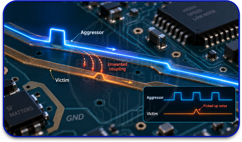
- Excessive Electromagnetic Coupling: Adjacent traces can exchange unwanted electrical energy through capacitive and inductive coupling. Insufficient spacing and long parallel routing increase the risk of crosstalk, particularly when high-speed or high-slew-rate signals are routed close together.
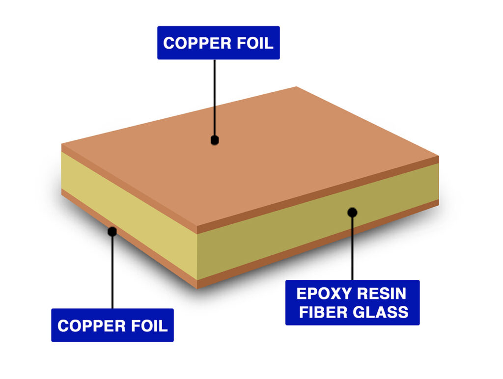
- Inappropriate Material or Stackup Selection: The PCB material and stackup directly influence impedance, propagation characteristics, and signal loss. Inconsistent dielectric thickness, unsuitable material properties, or poorly controlled layer geometry can make impedance difficult to predict and maintain.
- Power Distribution Network Noise: Changes in current demand can cause voltage fluctuations and ground bounce when the power-distribution network is not properly designed. Inadequate decoupling can increase supply noise, which may affect sensitive signal paths and reduce overall system stability.
Common PCB Signal Integrity Problems
Signal integrity problems appear as unwanted changes in a signal’s amplitude, waveform, noise level, or timing as it travels through the PCB. Common observable effects include:
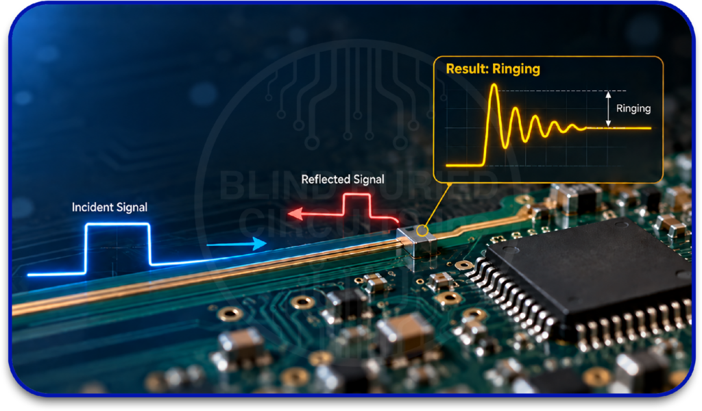
Reflections and Ringing: Reflections occur when part of a propagating signal is returned toward its source, while repeated reflections can produce ringing or oscillations around the intended signal level.
Crosstalk: Crosstalk is unwanted coupling from one signal path into another, introducing interference that can alter the voltage or timing characteristics of the affected signal.
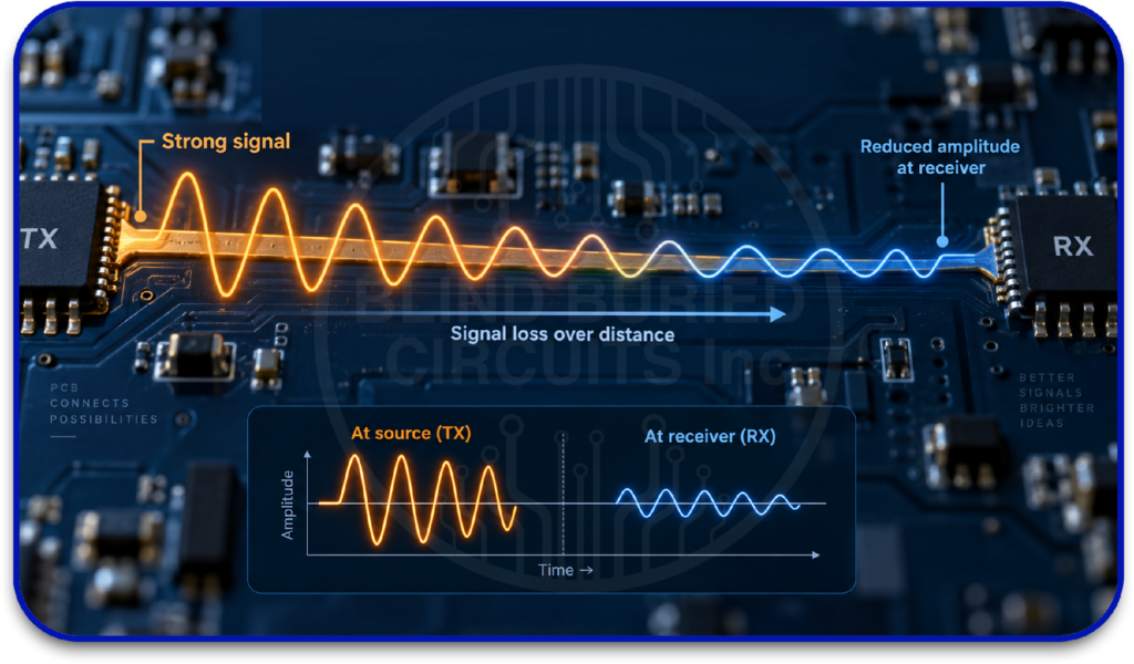
Signal Attenuation: Signal attenuation is the reduction of signal amplitude during transmission, particularly at higher frequencies, which can reduce receiver voltage margin and contribute to signal distortion.
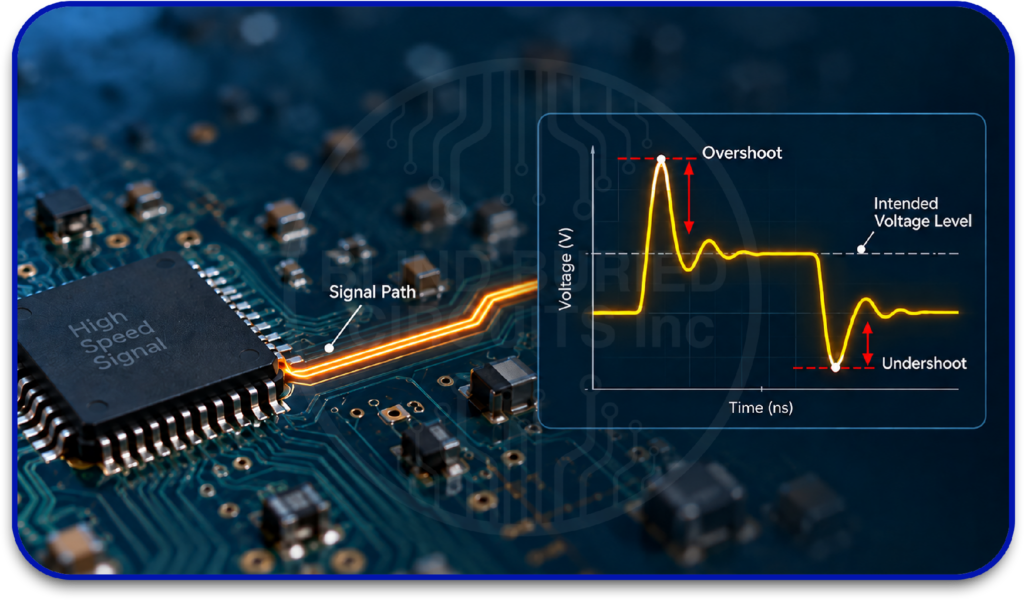
Overshoot and Undershoot: Overshoot and undershoot occur when a signal temporarily rises above or falls below its intended voltage level, potentially affecting receiver thresholds or stressing connected components.
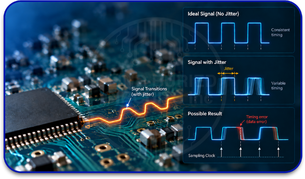
Jitter and Timing Errors: Jitter is unwanted variation in the timing of signal transitions, reducing available timing margin and potentially causing data errors when precise synchronization is required.
How PCB Layout Affects Signal Integrity
PCB layout helps determine how signals propagate through a circuit board. Routing decisions, layer transitions, component placement, and reference-plane management can directly influence signal quality, timing, and overall system performance.
- Trace Routing and Length: Trace routing affects both signal propagation and impedance consistency. Excessively long traces can introduce additional delay and signal loss, while unnecessary routing complexity can increase discontinuities and make signal behavior more difficult to predict. High-speed signals generally benefit from direct, well-controlled routing paths.
- Reference Plane Placement: Continuous reference planes help maintain predictable impedance and provide a low inductance return path for signal currents. Interruptions in the reference plane can alter current flow, increase noise, and affect overall signal quality, making proper plane placement an important aspect of PCB layout.
- Via Usage and Layer Transitions: Vias allow signals to transition between PCB layers but also introduce parasitic capacitance and inductance. Multiple layer transitions and unused via stubs can affect signal performance, particularly in high-speed designs. Careful via placement helps balance routing flexibility with electrical performance.
- Differential Pair Routing: Differential signals rely on two conductors carrying equal and opposite signals. Maintaining consistent spacing, routing symmetry, and appropriate length matching helps preserve differential performance and minimizes timing skew between the paired traces.
- Component Placement: The location of components influences signal-path length and routing complexity. Positioning transmitters, receivers, connectors, and other critical devices to support short and direct signal paths can improve signal quality and reduce potential routing challenges.
How to Identify Signal Integrity Issues
Identifying signal integrity issues requires a combination of simulation, measurement, and validation techniques. Detecting problems early helps engineers optimize PCB performance and reduce costly design revisions.
- Signal Integrity Analysis: Signal integrity analysis is typically performed during the design stage to evaluate how signals behave as they travel through PCB interconnects. Using simulation tools, engineers can assess factors such as impedance, reflections, crosstalk, propagation delay, and signal loss before fabrication, allowing potential issues to be identified and addressed early in the design process.
- Oscilloscope Measurements: Oscilloscopes are commonly used to validate signal behavior on fabricated prototypes. By observing real-time waveforms, engineers can identify abnormalities such as ringing, overshoot, undershoot, excessive noise, and timing variations that may affect circuit performance.
- Eye Diagram Analysis: An eye diagram provides a visual representation of signal quality by overlaying multiple signal transitions. The resulting “eye opening” helps engineers evaluate noise margin, timing margin, jitter, and overall signal integrity, making it a widely used tool for high-speed digital systems.
- Prototype Testing: Prototype PCB testing verifies PCB performance under actual operating conditions. Testing allows engineers to compare measured results with design expectations and confirm that the board meets its electrical, functional, and reliability requirements before full-scale production.
Practical Solutions to Improve PCB Signal Integrity
Maintaining signal integrity requires a combination of proper PCB design practices, careful routing strategies, and early design verification. The following approaches can help minimize signal degradation and improve overall board performance.
- Maintain Controlled Impedance: Design signal traces and PCB stackups to achieve the required impedance throughout the signal path. Consistent impedance helps reduce reflections and supports reliable signal transmission, particularly in high-speed applications.
- Provide Continuous Reference Planes: Place high-speed signal layers adjacent to solid reference planes whenever possible. Continuous planes provide a predictable return-current path and help maintain stable electrical performance across the PCB.
- Reduce Crosstalk: Increase spacing between adjacent signal traces and avoid unnecessarily long parallel routing. Proper trace separation helps minimize unwanted electromagnetic coupling between neighboring conductors.
- Optimize Via Structures: Limit unnecessary layer transitions and carefully manage via usage in high-speed signal paths. Techniques such as back-drilling or optimized blind and buried via structures can help reduce the effects of via-related discontinuities.
- Use Appropriate Decoupling Strategies: Place decoupling capacitors close to power pins and design an effective power-distribution network. Proper decoupling helps reduce supply noise and supports both signal integrity and power integrity requirements.
- Verify Designs Before Fabrication: Perform signal integrity analysis, simulation, and prototype validation before production. Early verification helps identify potential issues related to impedance, timing, crosstalk, and power-distribution performance, reducing the risk of costly redesigns.
Signal Integrity vs. Power Integrity in PCB Design
Signal integrity (SI) and power integrity (PI) address different aspects of PCB electrical performance, but they are closely interconnected in high-speed designs. SI focuses on the quality of signals traveling through interconnects, while PI focuses on maintaining stable power delivery to electronic devices.
|
Aspect |
Signal Integrity | Power Integrity |
|---|---|---|
|
Primary focus |
Quality of signal transmission | Stability of power delivery |
|
Main concern |
Signal distortion, reflections, crosstalk, loss, and timing variation |
Voltage fluctuations, power-distribution impedance, ripple, and transient response |
| Main paths analyzed |
Signal traces, vias, connectors, and transmission lines |
Power and ground planes, vias, decoupling networks, and power-distribution paths |
|
Typical analysis |
Impedance, reflections, crosstalk, eye diagrams, insertion loss, and timing |
PDN impedance, voltage ripple, transient response, resonance, and current distribution |
|
Design objective |
Deliver signals to the receiver within required voltage and timing margins |
Deliver stable voltage and current to devices under changing load conditions |
| Common mitigation | Controlled impedance, appropriate routing, reference planes, spacing, and optimized vias |
Decoupling capacitors, low-impedance power paths, suitable plane structures, and optimized PDN design |
How Signal Integrity and Power Integrity Interact
Although their primary objectives differ, SI and PI can influence each other. Variations in supply voltage or ground potential can affect signal thresholds and timing, while high-speed switching currents can introduce noise into the power-distribution network. Therefore, complex high-speed PCBs may require both signal integrity analysis and power integrity analysis to evaluate overall electrical performance.
Why Choose Blind Buried Circuits for Your PCB Project?
Blind Buried Circuits supports PCB manufacturing for designs where controlled electrical performance is important. Our capabilities include controlled-impedance PCB manufacturing, multilayer fabrication, blind and buried vias, and HDI PCB technologies. For high-speed designs, manufacturing review can help confirm stackup construction, impedance requirements, via structures and fabrication constraints before production.