

Objective
To explain PCB backdrilling, its role in reducing via stubs, and how it can support high-speed signal performance.
Key Takeaways
● Understand what PCB backdrilling is and why via stubs matter.
● Learn how the backdrilling process removes unwanted via barrel sections.
● Review key backdrilling design and manufacturing considerations.
● Understand where backdrilled PCBs may be used.
Table Of Contents
- Introduction
- What Is PCB Backdrilling and Why Does It Matter
- Why Do Via Stubs Matter in High-Speed PCBs?
- When Does a PCB Design Need Backdrilling?
- How Does the PCB Back Drilling Process Work
- How Does Back Drilling Improve High-Speed Signal Performance
- PCB Backdrilling Design Rules and Key Considerations
- Standard PCB Drilling vs. Back Drilling
- Benefits of Backdrilling in High-Speed PCB Design
- Common Applications of Backdrilled PCBs
- Build Reliable High-Speed PCBs With the Right Manufacturing Support
- Frequently Asked Questions
Introduction
As signal speeds increase, discontinuities in PCB interconnects can have a greater effect on signal integrity. Through-hole vias can contribute to this problem when their plated barrels extend beyond the layers required for a signal connection. The unused portion of a through-hole via is known as a via stub. Depending on its electrical length and the characteristics of the signal, a sufficiently long stub can introduce impedance discontinuities, reflections, and resonant effects that affect high-speed channel performance. PCB backdrilling can address this concern by modifying the via structure to limit the unwanted portion of the barrel.
This post explains what PCB backdrilling is, when it may be required, how the back drill process is applied to a PCB, how it can support high-speed signal performance, and the key design and manufacturing considerations engineers should evaluate.
What Is PCB Backdrilling and Why Does It Matter
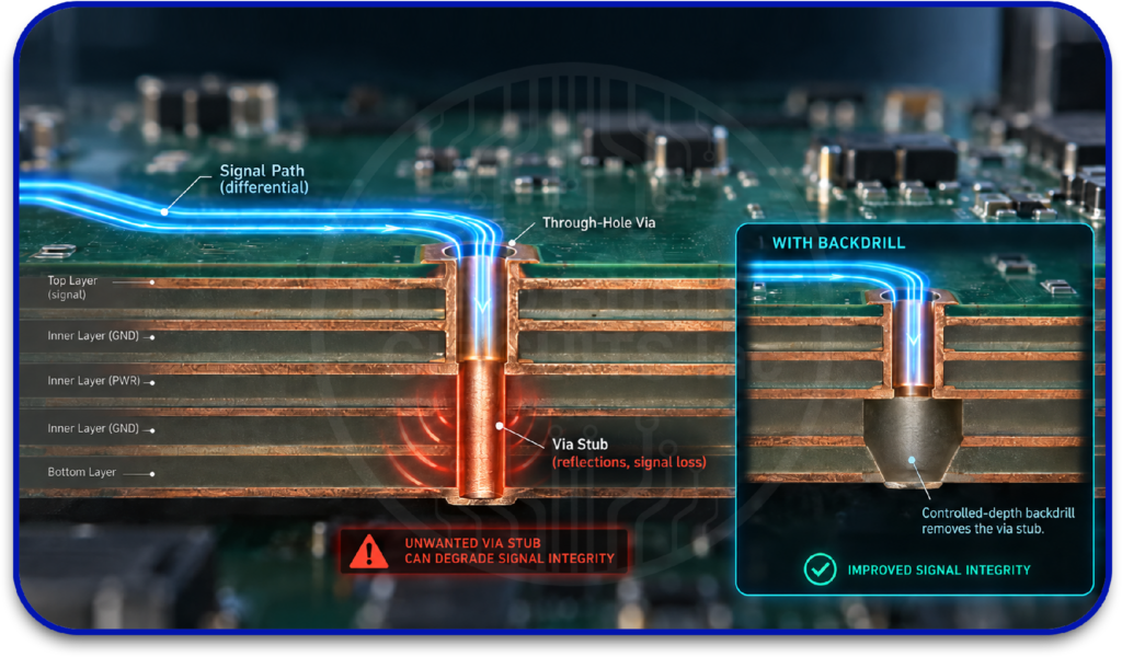
PCB backdrilling is a controlled-depth drilling technique used to remove the unused portion of a plated through-hole (PTH) via barrel. A through-hole via may pass through multiple PCB layers even when the signal only connects between specific layers. The part of the barrel extending beyond the signal connection is called a via stub. Although it is not part of the intended signal path, it remains part of the conductive via structure.
At high signal speeds, a sufficiently long via stub can introduce an electrical discontinuity, contributing to reflections and resonant behavior that may degrade signal quality.
Why Do Via Stubs Matter in High-Speed PCBs?
The electrical effect of a via stub depends on more than its physical length. Its significance is related to the stub’s electrical length relative to the bandwidth and rise time of the signal.
A short stub may have little practical effect on a particular channel, while the same physical stub could become significant in a higher-bandwidth design.
For this reason, there is no universal data-rate threshold at which every PCB requires backdrilling. Engineers should evaluate the complete interconnect, including the PCB stackup, via geometry, signal characteristics, channel length, and allowable signal-integrity limits.
Where a through-hole via creates a sufficiently significant discontinuity, reducing the stub length can improve the predictability of the channel response.
When Does a PCB Design Need Backdrilling?
The need for backdrilling depends on the board’s construction and interconnect requirements. Several design conditions can indicate when it is worth evaluating:
High-speed signal paths: Backdrilling may be appropriate for demanding high-speed channels where through-hole vias introduce stubs that could affect the required signal performance.
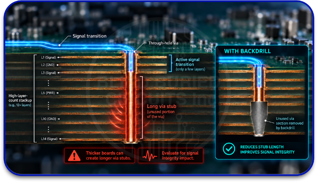
Thick or high-layer-count boards: A through-hole via can span substantially more of the board than the signal connection requires, potentially leaving a longer stub that warrants evaluation.
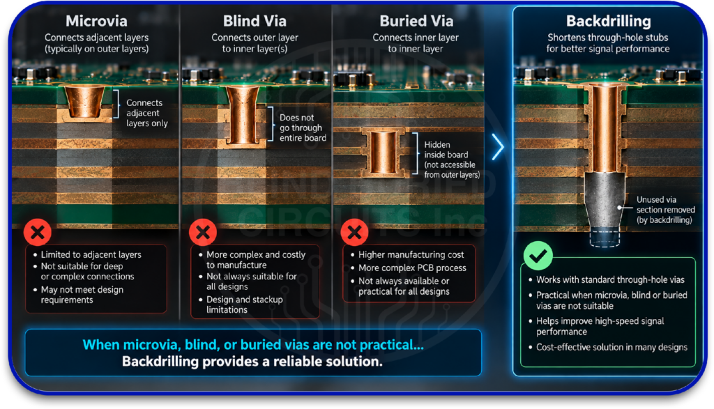
Alternative via structures is less suitable: Backdrilling can provide a practical way to shorten through-hole stubs when blind, buried, or microvia structures do not meet the design, manufacturing, or cost requirements.
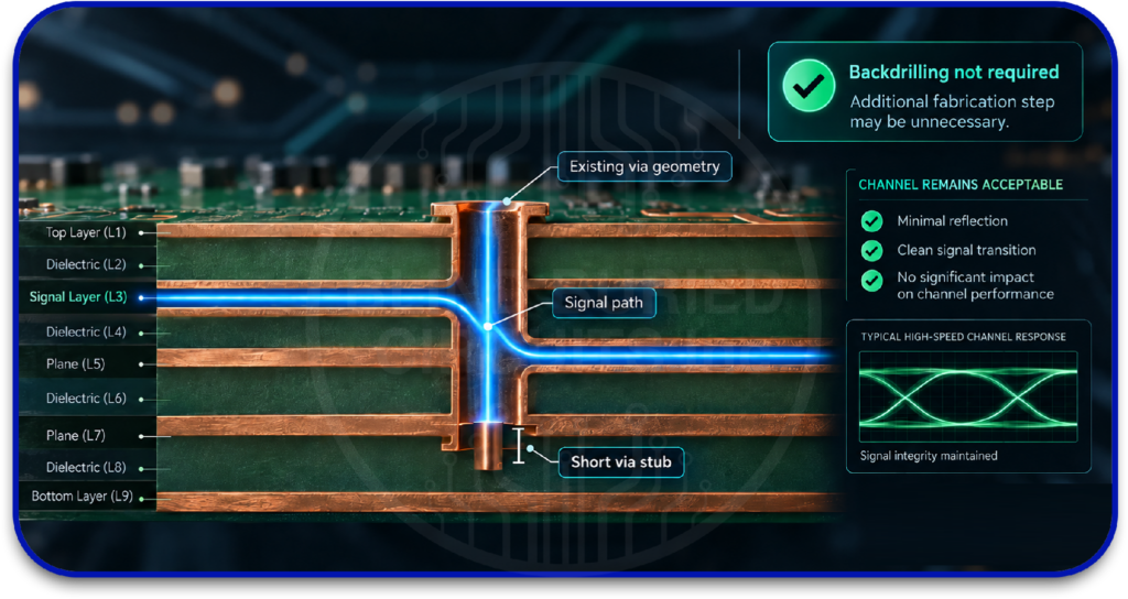
Stub effects are negligible: Backdrilling may offer little value when the existing via geometry does not create a stub that is significant for the intended channel, making the additional fabrication step unnecessary.
How Does the PCB Back Drilling Process Work?
A backdrill operation is planned from the via geometry and layer configuration, then carried out with controlled drilling equipment. The main steps include:
- Identify the required vias: Determine which through-hole vias require stub removal and which barrel sections need to be removed.
- Specify the drilling parameters: Define the entry side, drill diameter, specified backdrill depth, and stop layer for each selected via based on the board construction.
- Specify the drilling parameters: Define the drilling side, backdrill diameter, target depth and required residual stub based on the signal-layer PCB transition and PCB stack-up.
- Perform the backdrill operation: Use a larger secondary drill from the selected board surface to remove the unwanted plated barrel section.
- Control the drill depth: Stop the operation at the specified depth to preserve the portion of the via required for the intended electrical connection.
- Verify the finished board: Check the backdrilled vias to confirm that their location, depth, and remaining stub meet the PCB design and fabrication requirements.
How Does Back Drilling Improve High-Speed Signal Performance
A through-hole via can extend beyond the layers used by a signal, leaving an unused section of conductive barrel. In a high-speed interconnect, this stub creates an additional electrical path that can disturb the intended transmission-line behavior. When its electrical length becomes significant relative to the signal, it can contribute to impedance discontinuities, reflections, and resonant effects that distort the transmitted waveform.
Backdrilling reduces these effects by shortening the stub and limiting its electrical influence. This can help high-speed channels maintain more predictable behavior. The extent of the improvement depends on the original stub length, signal characteristics, and the design of the complete interconnect.
PCB Backdrilling Design Rules and Key Considerations
A back drill PCB design must balance the electrical requirements of the interconnect with the physical limits of the fabrication process. Key considerations include:
- Residual stub length: Set an acceptable remaining stub length based on the signal requirements and channel characteristics. Shorter stubs generally reduce their electrical impact, but tighter limits can increase fabrication difficulty and cost.
- Backdrill diameter: The backdrill uses a larger diameter than the original via hole to remove the unwanted barrel section. The backdrill diameter must provide adequate clearance from surrounding copper features.
- Backdrill depth and tolerance: Define the entry side and stop depth carefully so the drill reaches the intended termination point without removing copper needed for the electrical connection. Manufacturing and material tolerances must be included when establishing this depth.
- Via and pad geometry: Review the complete padstack, including hole size, pads, and unused pads along the drilling path. The enlarged backdrill must not interfere with features that remain functional.
- Clearance requirements: Allow sufficient space between the backdrill and nearby traces, planes, pads, and other vias. Because the backdrill is larger than the original hole, its clearance requirements must be considered separately.
- Layer transitions: Identify the layers where the signal enters and leaves the via so the backdrill can be positioned to remove only the unnecessary barrel section.
- Board thickness and material construction: Account for the board’s layer and dielectric construction when establishing backdrill depth, while allowing for fabrication variation.
- Fabrication capabilities and DFM requirements: Confirm the manufacturer’s capabilities for drill diameter, depth control, tolerances, and drill-to-copper clearance before finalizing the design. Backdrilling requirements should be incorporated into the DFM review and manufacturing documentation.
Standard PCB Drilling vs. Back Drilling
Backdrilling and standard PCB drilling serve different purposes in via fabrication. Standard drilling creates the original hole used to form a plated through-hole (PTH) via, while a back drill PCB process subsequently modifies selected vias by removing part of the plated barrel. The key differences are:
| Standard PCB Drilling | Backdrilling |
|---|---|
Creates the original hole used to form a plated through-hole via. | Modifies an existing plated through-hole via by removing part of its barrel. |
For a conventional through-hole via, the drill passes through the board to create the required hole. | Uses controlled depth to remove a selected barrel section. |
Establishes the complete plated barrel. | Leaves the functional portion of the barrel intact. |
Provides the physical structure for the via connection. | Removes the specified excess barrel section. |
Benefits of Backdrilling in High-Speed PCB Design
Backdrilling can offer practical design flexibility when through-hole vias remain necessary but their full barrel length is not required for the connection.
- Preserves through-hole structures: Allows designers to retain through-hole vias where the board architecture requires them.
- Provides an additional interconnect option: Gives engineers another approach to consider alongside blind, buried, and microvia structures.
- Supports selective application: Allows stub reduction to be applied where the electrical requirements justify the additional operation.
- Accommodates complex multilayer designs: Can be incorporated where through-hole connectivity remains part of the required board construction.
Common Applications of Backdrilled PCBs
Backdrilling is commonly considered in systems that combine demanding high-speed interconnects with through-hole vias. Typical applications include:
- Networking equipment: Switches, routers, and related hardware with high-speed data interfaces.
- Telecommunications equipment: Communication hardware that relies on demanding high-speed connections.
- Data center and computing hardware: Servers and computing platforms with high-speed interfaces.
- Backplane-based systems: Equipment that uses high-speed connections between boards or modules.
Build Reliable High-Speed PCBs With the Right Manufacturing Support
A strong PCB design depends on how effectively its requirements are translated into a manufacturable product. An experienced PCB manufacturing partner can help engineering teams evaluate stackup requirements, via structures, drilling parameters, tolerances, and other fabrication constraints before production. Blind Buried Circuits supports complex PCB fabrication and PCB assembly for demanding electronic applications, including advanced multilayer PCB technologies, HDI structures, blind and buried vias, and backdrilling capabilities for high-layer-count applications. Contact our team today to discuss your requirements.